HF Receiver Mark I
This was my fist attempt at building a decent shortwave receiver that offers the most important amenities and is easy to operate. By now I have designed and built an improved predecessor which is described here. That version uses the same basic principles, therefore this description will be brief. For more details follow the link to the predecessor.
This design has been first presented on mikrocontroller.net in this thread.
Overview
The receiver covers a frequency range from 10 kHz to 30 MHz (tuning range starts at 1 kHz), and detects AM (synchronous) as well as SSB (upper and lower sideband, with sideband selectivity). The two LO and the BFO are synthesized from a precise TCXO time base; tuning is by an optical rotary encoder with a minimum resolution of 10 Hz; the BFO offset range is from 0 Hz to ±3.5 kHz with 1 Hz resolution. The AGC can be switched between fast, slow and hanging (fast attack and slow release) mode, or manual (gain selectable by front panel knob). Three IF bandwidths (filter setup 2.7 kHz, 10 kHz, 12 kHz—clearly not a very good choice of bandwidths, but that's what my junkbox had to offer at the time of construction) can be selected electronically. A RSSI indication is provided by means of a readout in dBm of the signal level present at the antenna input on a dedicated front panel display. In manual gain control mode this display indicates the approximate demodulator use in percent. A simple squelch with threshold selectable in dBm is provided, which also triggers a rear panel open collector COR output. Moreover, there is a selectable 20 dB input attenuator, a headphones jack and a line audio output. For more detailed data see this pdf file.
The complete design data is provided as a zip archive. It contains the schematics and board layouts which, were designed with Eagle 7.7.0—the last version before Cadsoft Computer Pleiskirchen sold their only product to Autodesk and folded. Due to the licensing policy of Eagle's new owners I have, like many others, migrated to KiCad in the meantime. Also included are the front and rear panel design files as well as the design file for the display filter acrylic panel, which were manufactured by Schaeffer AG and designed with their Software “Frontplatten-Designer”. The firmware source code and the binaries are included as well.
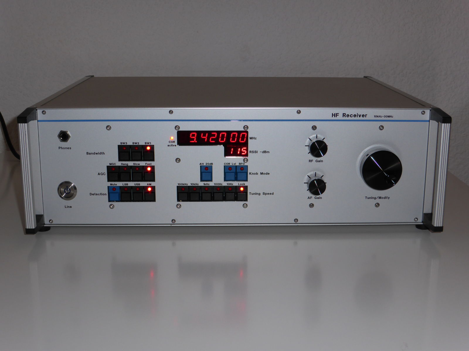

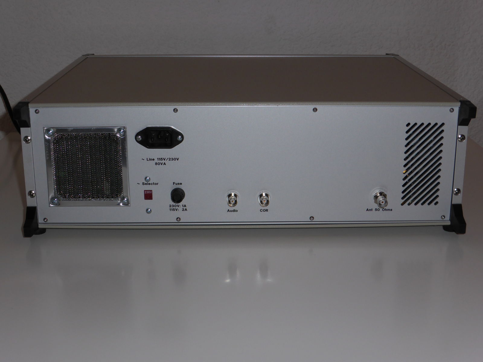

Construction
The receiver is housed in a 19" rack enclosure which is three rack units high. It was chosen because it was cheaply available in used condition; I don't know the manufacturer, but it could be Knürr. All PCBs are bolted to a massive 3 mm aluminium panel located at the bottom of the case which also facilitates a low impedance ground return. Most of the cabling (except coax and ribbon) is routed below the panel and passes through rubber grommets.
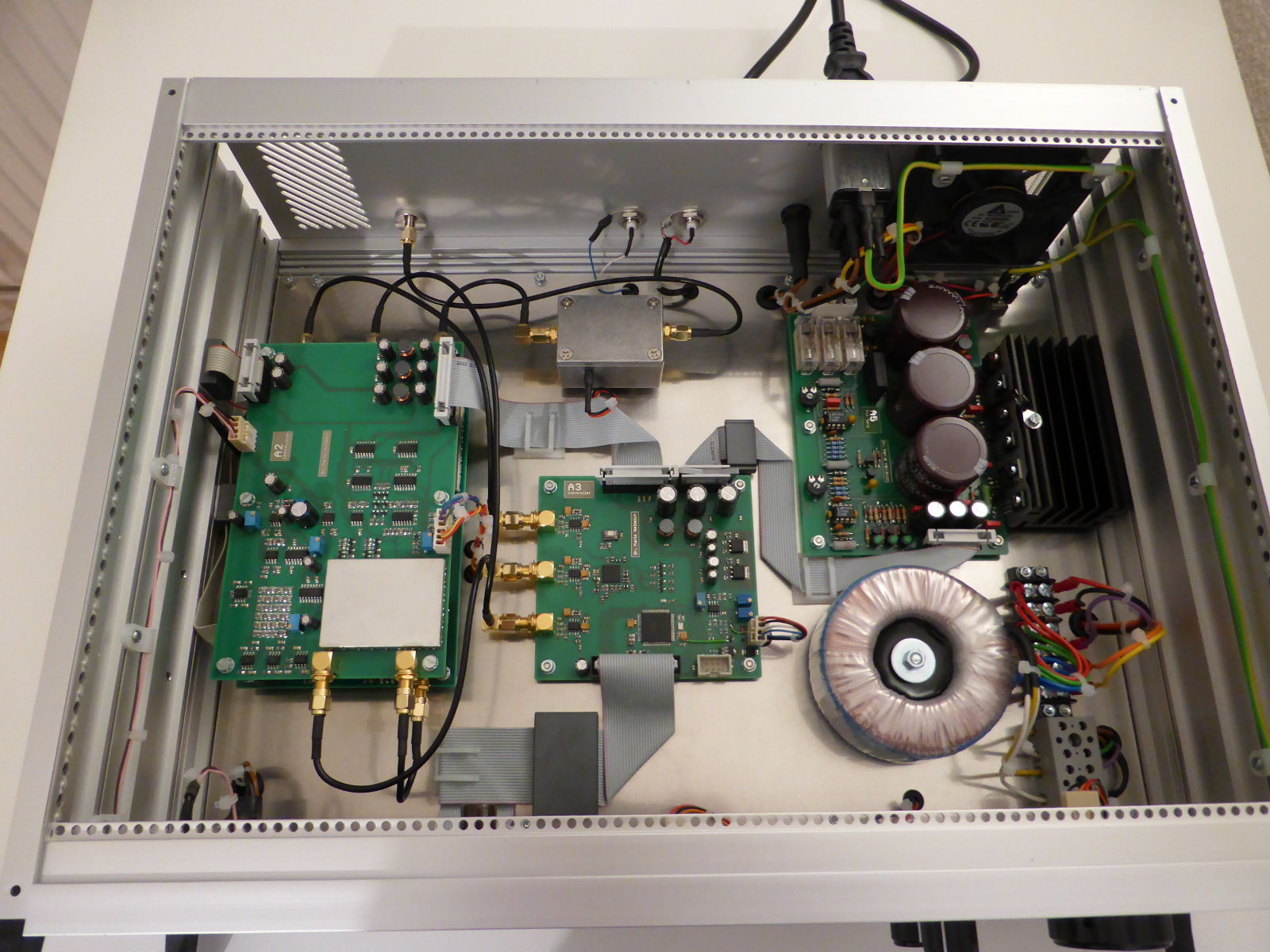

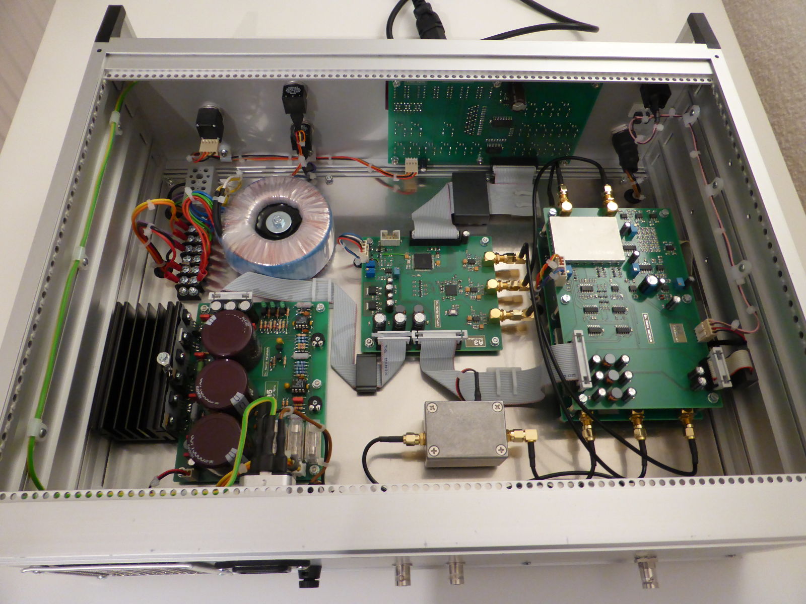

To achieve a somewhat modular construction with individually testable building blocks the circuit is distributed over six PCBs which are designated A1 to A6:
- A1 Converter board: contains the first and second mixer, IF filters and amplifiers
- A2 Demodulator board: contains the demodulator and audio circuitry
- A3 Control board: contains the microcontroller as well as the synthesizer and TCXO
- A4 Front panel board: contains LED displays and pushbutton switches
- A5 Power supply: the linear power supply
- A6 Attenuator: contains the 20 dB switchable attenuator
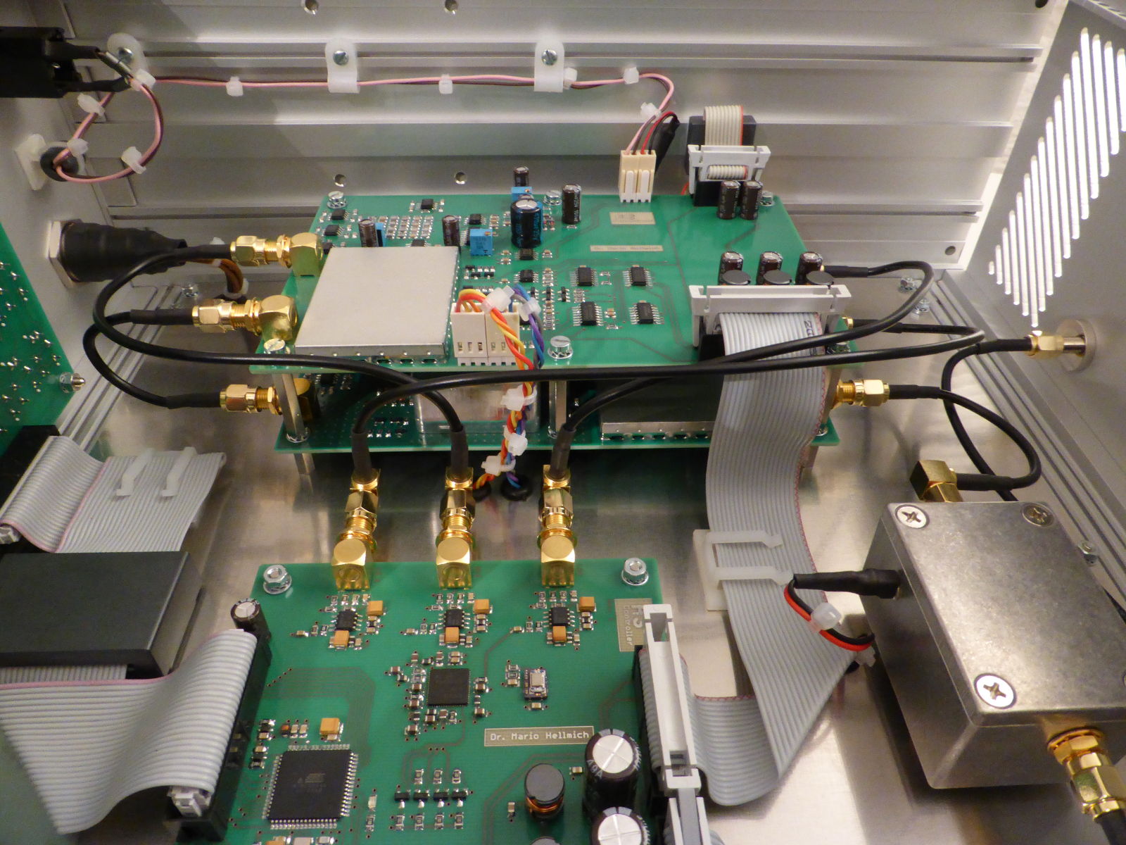
The two boards A1 and A2 are stacked to save some space. The attenuator A6 is in its own little shielded die cast aluminium box (manufactured by Hammond), which is penetrated by SMA jacks and a feedthrough capacitor for the control line.
Circuit diagrams and block diagram
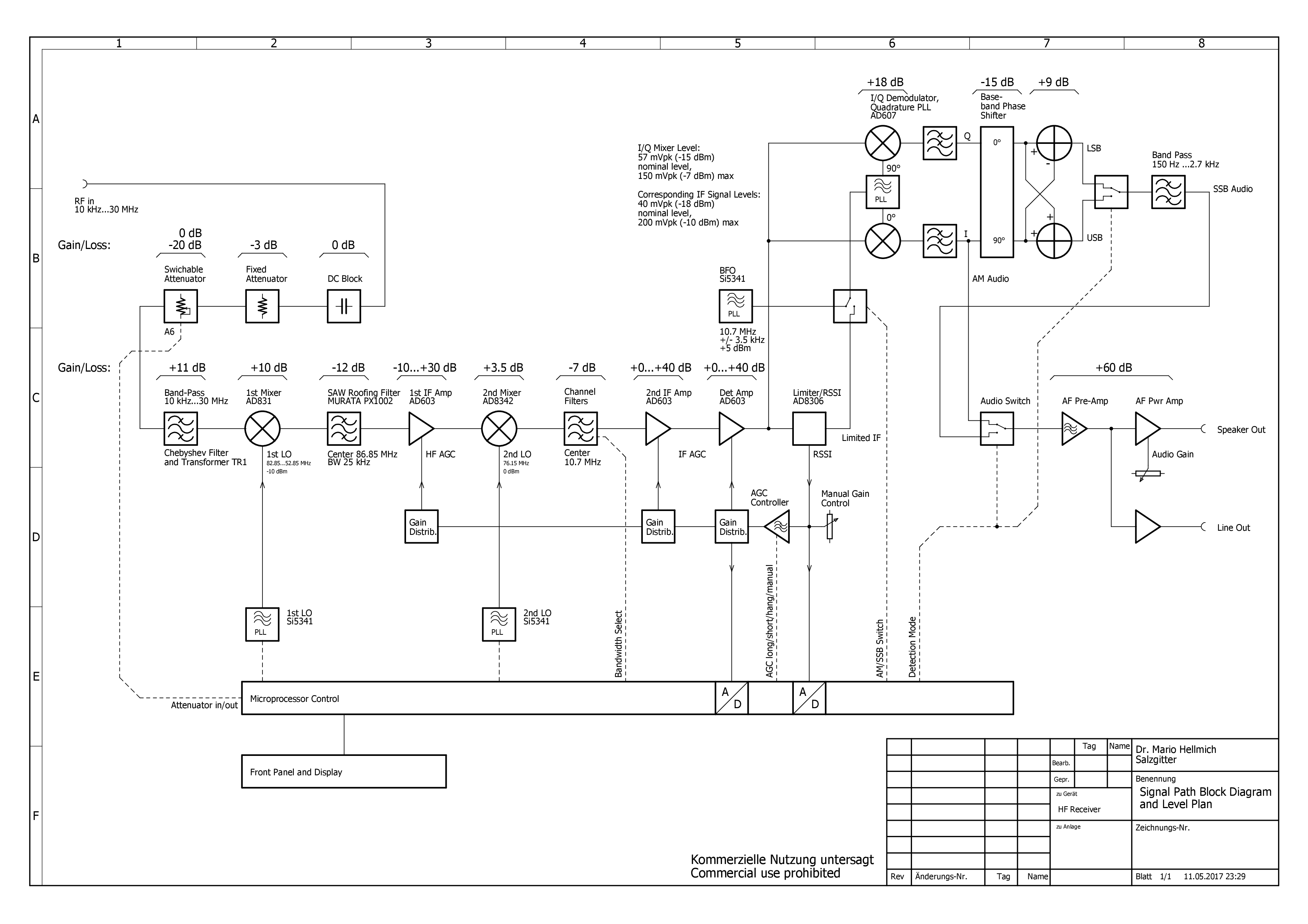
For an overview of concept see the block diagram below. The complete schematics can be downloaded as a pdf file. As mentioned before I will only provide brief description of the circuit in the following since it is conceptually somewhat similar to and has been superseded by its predecessor.

A1 Converter
The first mixer is an AD831 active Gilbert cell mixer made by Analog Devices, whose balanced input is matched to 50 Ohms single ended by a transformer. This transformer provides a few dB of practically noiseless gain, which makes the receiver quite sensitive. Of course, this amount of gain together with a Gilbert cell mixer impairs the large signal handling capabilities. See below for more remarks on this point and test results. The roofing filter at the first IF of 86.85 MHz is a low loss SAW filter. This is followed by the first active gain stage, an AD603 VGA, and the second mixer, an AD8342, which translates to the second IF of 10.7 MHz. Then follow the three crystal channel filters, which are switched by PIN diodes, and the second IF amplifier (two AD603 in cascade).

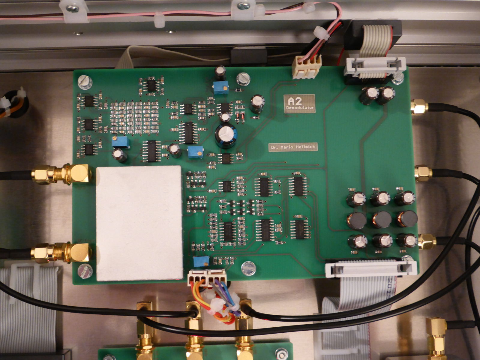
A2 Demodulator
This board contains the synchronous AM and SSB demodulator, which is built around an IQ mixer and an associated quadrature PLL oscillator for AM carrier recovery, in conjunction with an AD8306 limiter. The SSB detector works according to the phasing method, where the sideband selectivity is achieved by a polyphase filter of discrete design at baseband. Electronic analog switches select the operating modes of the demodulator. The AGC circuits are also located on this board, which use the AD8306 as a detector to control the second IF signal level. For noise figure optimization the AGC acts sequentially between first and second IF and only increases the gain in the second IF if the gain in the first IF is at maximum.

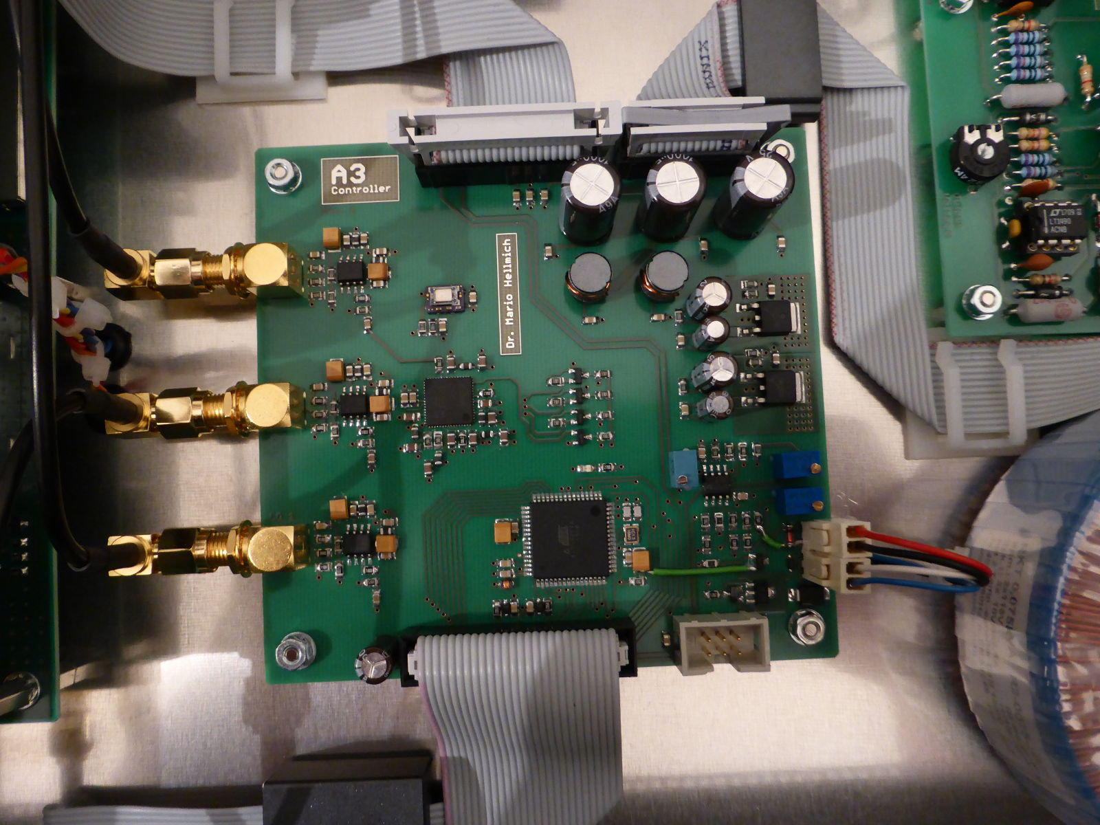
A3 Control board
The receiver is controlled by an ATmega64A microcontroller clocked at 16 MHz. The microcontroller drives the display and status LEDs, polls the keyboard and the rotary encoder, provides various control signals to the other assemblies, measures RSSI and gain set voltages to calculate and display the signal level at the antenna input in dBm, and controls the PLL chip through I²C bus. The PLL chip is a Si5341 ultra-low phase noise clock generator, which generates the first and second LO and the BFO signals. It is referenced to a precise 0.28 ppm TCXO. Two linear regulators with 3.3 V and 1.8 V outputs power the PLL chip.

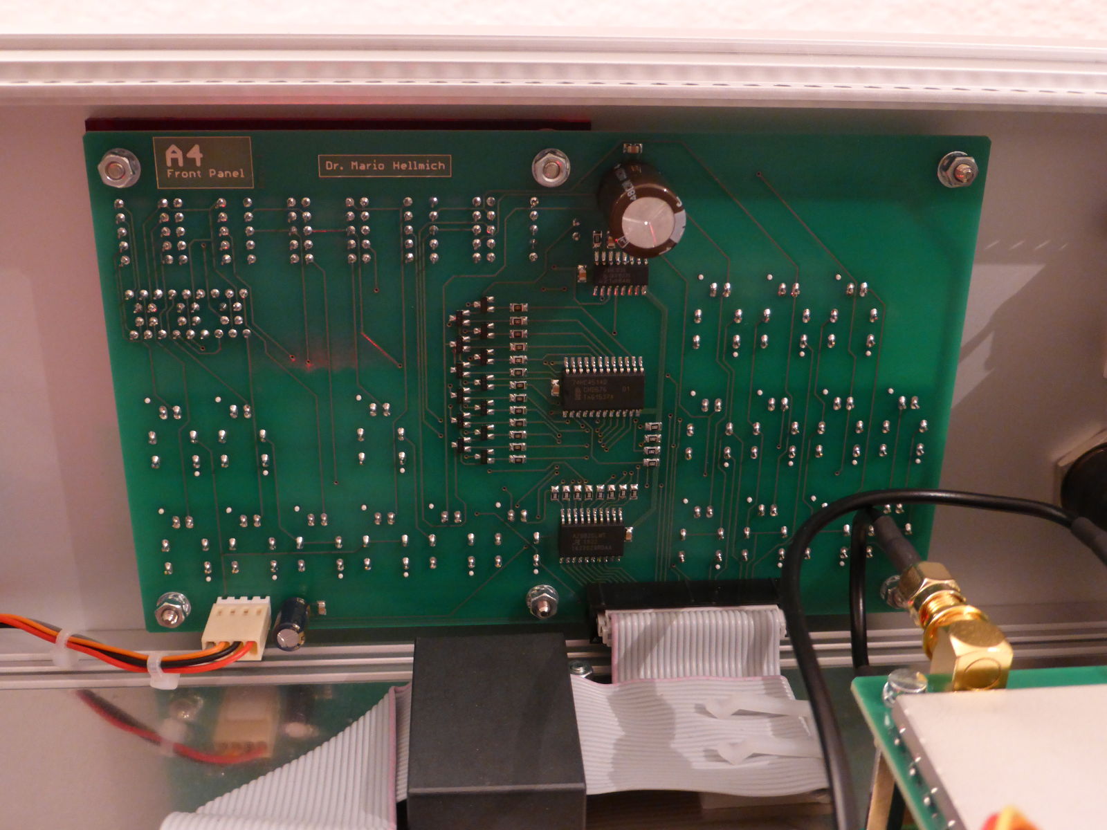
A4 Front panel board
This is the front panel board with LED displays and pushbuttons with status LED indicators. This board also passes the signal from the rotary encoder on to A2. The rotary encoder is an optical one manufactured by Bourns (model ENA1J-B28-00128L) with 128 steps per revolution.

A5 Power supply board
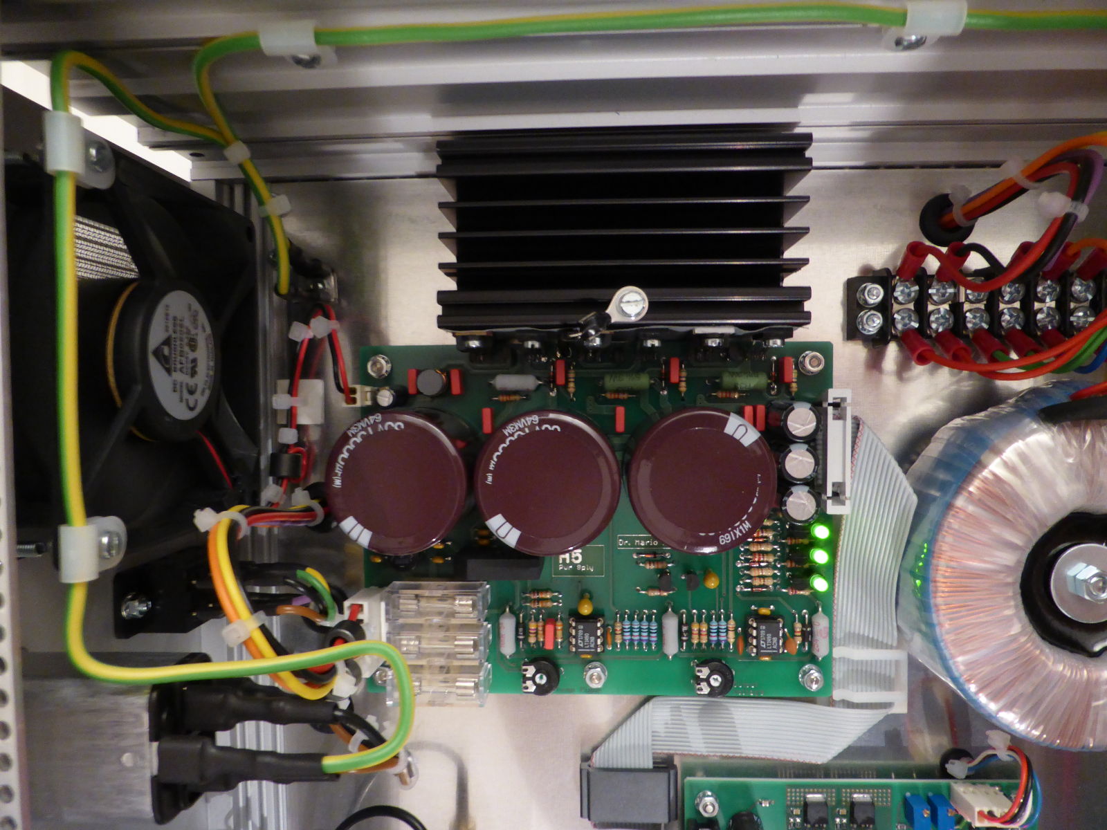
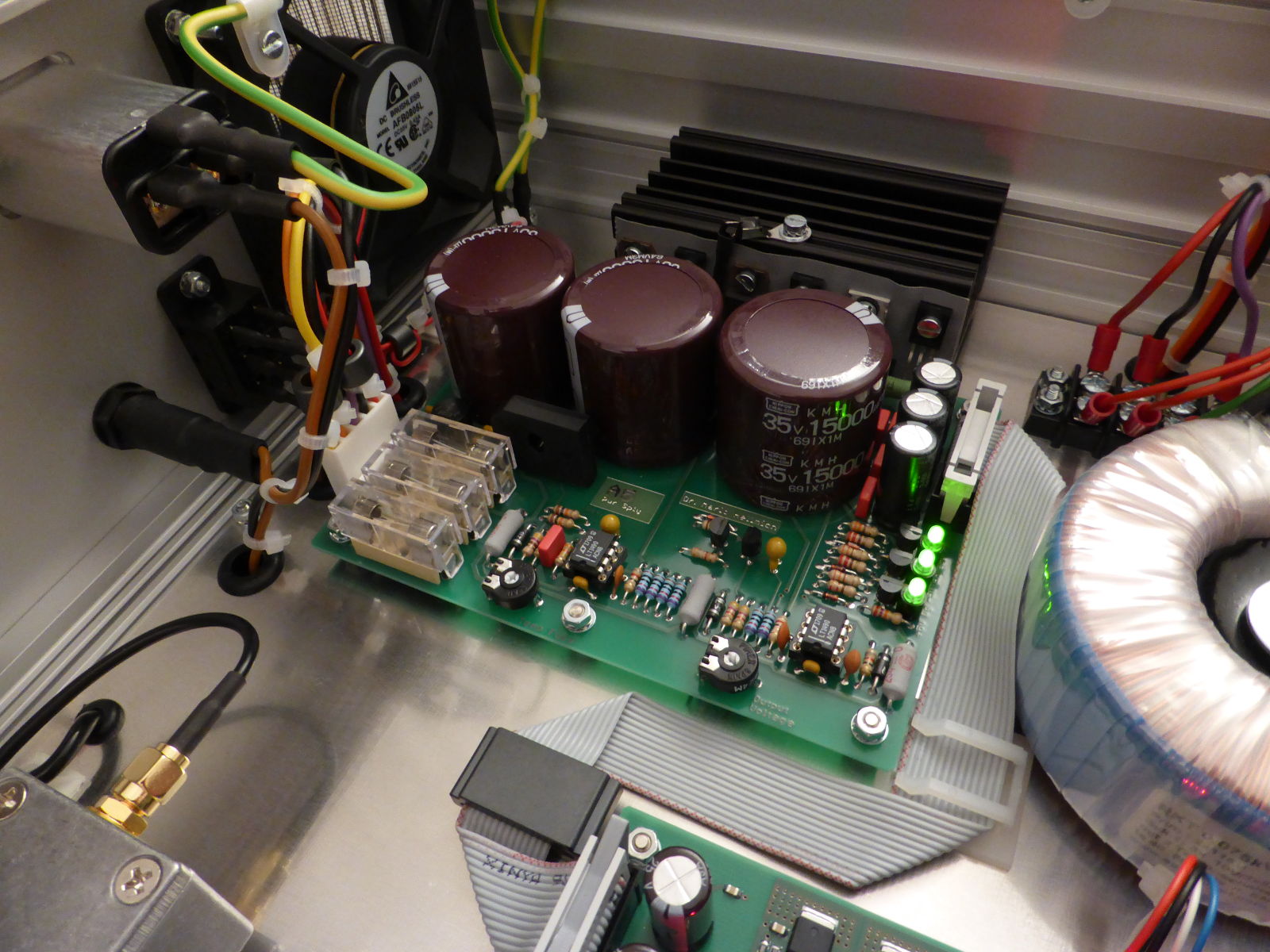
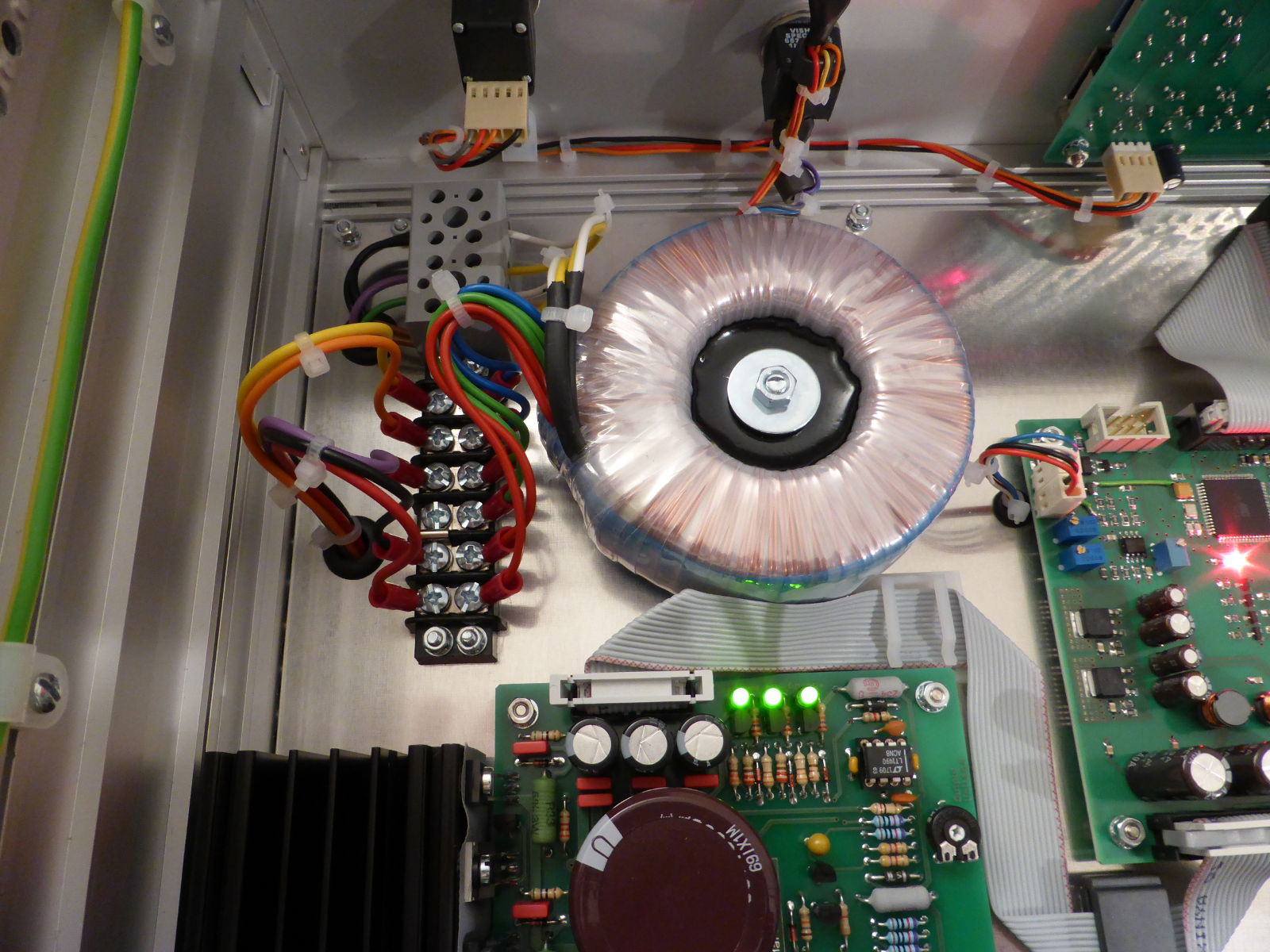
The power supply is a fairly standard linearly regulated supply and powers three voltage rails: +5 V digital, +5 V analog, and −5 V analog. All output voltages are referenced to the +5 V analog rail. There is an overcurrent protection and a crowbar circuit for each rail, and a thermal cutout.
The toroidal transformer with two primary and three secondary windings has been custom manufactured for this receiver.



Performance
Some performance test data is reported in this pdf file. As already remarked, the design with the active Gilbert cell as first mixer and additional gain in front is, in view of the requirements for a shortwave receiver, not very linear, even though the AD831 definitely qualifies as a “low distortion mixer”, as the datasheet advertises it. This is reflected in an antenna input referred third order intercept point (TOI) of about 5 dBm at 100 kHz spacing between the tones that I obtained in a two-tone measurement. The datasheet TOI value of the AD831 is 24 dBm, but this is output referred. With the gain in front of the mixer and the post mixer amplifier configured for additional gain the TOI of 5 dBm with reference to the antenna input are plausible. Even though this may not be a particularly good value, it will yet be sufficient for many receiving situations with not too efficient antennas. If problems occur, the 20 dB attenuator can be switched in which will improve the TOI to about 25 dBm, at the expense of sensitivity.
