HF Receiver Mark II
This was my second attempt at building a high performance analog shortwave receiver. The first attempt has been presented here. It is really only a reimplementation of the earlier version along the same principles, but with a number of improvements. The motivation to build it was mainly to replace the frontend of the earlier version by a newly designed one with better large signal immunity, to make some minor upgrades, and to add some features. Just as its predecessor this receiver implements a classical design, i.e., a double conversion superhet with a high first IF and completely analog signal processing, but realized with modern components, non of which was EOL or discontinued at the time of design (circa end of 2018). The 80s style operating concept and front panel design with pushbuttons and seven segment LED displays is classical as well.
This design has been first presented on mikrocontroller.net in this thread.

Overview
The receiver covers a frequency range from 10 kHz to 30 MHz (tuning range starts at 1 kHz), features a synchronous AM demodulator, a sideband-selective SSB demodulator, and a narrow-band FM demodulator. It is equipped with a simple 6-band preselector, a preamplifier (temporarily not used—see below), and with a selectable 20 dB input attenuator. The three LOs and the BFO are synthesized and referenced to a precise TCXO time base. Tuning is by an optical rotary encoder as well as by direct frequency entry via keypad. The encoder tuning resolution can be selected between 1 Hz (the minimum tuning resolution) and 10 kHz by dedicated front panel buttons. The BFO offset range is from 0 Hz to ±3.5 kHz with 1 Hz resolution, and can selected by rotary encoder (with selectable tuning resolution) or by direct keypad entry. The AGC can be switched between fast, slow and hanging (fast attack and slow release) mode, or can be set to manual (gain selectable by front panel knob). Four IF bandwidths (500 Hz, 2.4 kHz, 5 kHz, 15 kHz) can be selected electronically; the corresponding channel filters are high quality multi-pole crystal filters. A RSSI indication is provided by means of a readout of the signal level in dBm present at the antenna input on a dedicated front panel display. In manual gain control mode this display indicates approximate demodulator use in percent. A simple squelch with threshold selectable in dBm is provided, which also operates a rear panel open collector COR output. An internal speaker (can be switched on or off separately), a headphones jack and a line audio output are provided. The volume control only operates on the speaker and headphones. An IF monitor output at 10.7 MHz with a level of about −30 dBm is provided. For more detailed data see this pdf file.
The complete design data is provided as a zip archive. It contains the schematics and board layouts which were designed with KiCad. The design files included in the zip archive were drawn with KiCad version 4.0.7, but should also work with the current version 5. Also included are the front and rear panel design files along with the design file for the display filter acrylic panel, which were all manufactured by Schaeffer AG from Berlin and designed with their Software “Frontplatten-Designer”, which is available for download from their website and can be used free of charge. Moreover, the archive contains the firmware source code (written in C) and as well as binaries. The boards were all manufactured by LeitOn from Berlin.
Construction
The receiver is housed in a 19" rack enclosure manufactured by Schroff, which is two rack units high, and which is equipped with an optional tilting bail. All the innards are mounted on a 1 mm aluminium panel which also facilitates a good ground connection for the circuit boards.


The receiver is built on five boards which are labeled A1 to A5:
- A1 Analog board: contains the main part of the receiver and all analog signal processing
- A2 Control board: contains the microcontroller as well as the synthesizer and TCXO
- A3 Front panel: contains LED displays and the pushbutton switches
- A4 Power supply: mains transformers and the linear power supply
- A5 Preselector: the 6-band preselector
Circuit diagrams and block diagram
The block diagram provides an overview of the receiver and shows its principle of operation. In the following I will provide a more detailed description of the circuit moving along the signal path from the antenna input to the audio circuits. The complete schematics of the receiver can be downloaded as a pdf file.

A1 Analog board
The antenna signal is fed from the preselector A5 into the input jack A1-J2. After an input protection circuit consisting of a 75 V spark gap, two RF clamping diodes and an optional light bulb (if you are really paranoid about input protection) the signal reaches the 20 dB attenuator, which can be switched into the signal path by two RF reed relays. Then follows the image rejection filter with 32 MHz corner frequency and the switchable preamplifier A1-U4, which is realized with a Mini-Circuits Gali-74+ MMIC. The preamp is currently not fitted as I have been too clumsy to install the reed relays in the correct way. Moreover, it turned out that the LO re-radiation causes some problems for the Gali-74+, so that some more tweaking is needed here. On the other hand, a sufficiently sensitive HF receiver does not really need a preamp unless you operate it with a very weak antenna, so that fixing this issue is not a priority.
Next follows the fist mixer, which is realized as a so-called H mode mixer. The switching elements are two a video bus switches A1-U2 and A1-U3 (74LVC1G3157 by NXP); the LO signal is transmitted as LVDS from A2 and is received on A1 by a DS90C402 dual LVDS receiver (A1-U1A) from Texas Instruments. Together with the Mini-Circuits T2.5-6T-KK81+ signal transformers (A1-T1, A1-T2, A1-T3) this makes a mixer with good linearity. This mixer translates to the first IF frequency of 86.85 MHz. It is followed by the roofing filter, consisting of two low-loss narrowband SAW filters A1-Y1, A1-Y2 (PX1002 by Murata) with 25 kHz bandwidth. Originally these are intended for TDMA IS-54 receiver IF applications in the D-AMPS mobile phone system. These two filters are interconnected with two quadrature hybrid couplers ADQ-90+ by Mini-Circuits in order to present a frequency independent load impedance of 50 Ohms to the mixer.
Next in the signal path follows the first gain stage A1-U5, a PSA4-5043+ low noise amplifier by Mini-Circuits, which has a noise figure of about 0.7 dB at the IF frequency. This amplifier is followed by a variable gain amplifier A1-U5 (AD603 by Analog Devices) with 40 dB adjustment range, configured to provide a gain between −10 dB and +30 dB. Then comes the second mixer A1-U7, an AD831 highly linear active Gilbert cell mixer by Analog Devices, which translates to the second IF of 10.7 MHz. The AD831 was used as the first mixer in the previous version of this receiver.
At 10.7 MHz the channel filtering is performed by four selectable high quality multi-pole crystal filters manufactured by Krystaly Hradec Králové from the Czech republic. The filters are switched by PIN diodes into the signal path. The control signals for the PIN diodes and their proper blocking and filtering is critical. Moreover, the board layout must ensure that crosstalk between filter input and output through the control lines is well below the stopband attenuation of the filters (which is in excess of 90 dB). For the bandwidths and number of poles of the filters fitted see the pdf containing the specifications, which is linked above. The filters are followed by the second IF variable gain amplifiers A1-U9 and A1-U10, which are again AD603, configured in cascade to provide a total gain between 0 dB and 80 dB. They operate in sequential mode, i.e., the gain of the second amplifier is only increased after the gain of the first has reached its maximum. Moreover, a buffer amplifier provides a sample of the second IF signal to a rear panel BNC connector.
The SSB and synchronous AM demodulator is built around an IQ demodulator. For this purpose the AD607 receiver IF subsystem IC (A1-U13) by Analog Devices is employed, from which only its IQ mixer and its PLL quadrature oscillator are used. In order to achieve AM carrier recovery, a limiting amplifier A1-U11 (AD8306 by Analog Devices) feeds the limited IF signal (while conserving its phase relation) to the quadrature PLL of the AD603, which locks to it. In fading conditions the PLL will tend to maintain its frequency, which helps to stabilize the demodulator even under difficult receiving conditions. The AD8306 also serves as level detector for the AGC and the front panel RSSI display. In AM mode the IQ mixer translates the IF signal to baseband for detection. SSB detection works according to the phasing method, where sideband selectivity is achieved by a broadband polyphase filter at baseband, realized with discrete components. There is a lot of information online about the design and manufacture of broadband polyphase filters. For good unwanted sideband rejection low tolerance resistors and C0G capacitors, selected for equal capacitance, are used. The switchover between the different demodulation modes (AM, USB and LSB) is achieved by analog switches and a PIN diode switch, which either routes the limited IF or the BFO to the PLL input of the AD607.
The narrow band FM demodulator A1-U21 is realized with a SA605 made by NXP. In FM mode the IF signal limited by A1-U11 is translated to 455 kHz, then filtered by two Murata ceramic filers and demodulated by the quadrature demodulator section (coincidence FM detector) of the SA605.
The AGC circuits are built around A1-U24. As already mentioned, the AGC control loop uses A1-U11 as sensing element for the control parameter, i.e., the second IF level. The AGC can be switched electronically between fast, slow, and hanging (fast attack and slow release time) mode, and can be set to manual (gain adjustable by front panel knob). For noise figure optimization the AGC acts sequentially between first and second IF: the gain in the second IF is only increased if the gain of A1-U1 in the first IF has reached its maximum.
Moreover, the audio signal switching and conditioning is performed on A1. There are two power amplifiers, one for the internal speaker and the other for headphones output, both realized with a LM4857 by Texas Instruments, which are 750 mW integrated audio amplifiers with DC volume control. The front panel volume adjust acts on both speaker and headphones; the internal speaker can be turned off by a pushbutton. If no detection mode is selected by a front panel switch, the audio is muted. A line audio output with a separate buffer amplifier is provided. A 100 nF capacitor at the headphones jack in parallel to the output and another 10 nF capacitor in parallel to the headphones connector on the A1 board has been added in order to calm the amplifier and to avoid interference by parasitic signals picked up by the headphones cord.

A2 Control board
The receiver is controlled by an ATmega64A microcontroller A2-U10, which is clocked at 16 MHz. A2-U10 drives the front panel (LED display, status LED indicators in the pushbuttons and front panel LED's, keyboard and rotary encoder polling), and controls a shift register with latch (A2-U11, A2-U12, A2-U13), which provides control signals for the analog section A1 of the receiver. Moreover, the PLL circuit is controlled by A2-U10 via I²C bus. Finally, A2-U10 measures the RSSI and gain set voltages present on A1 in order to calculate the signal level present at the antenna input in dBm. The op-amp A2-U8 performs some signal conditioning, and A2-U9 is the reference voltage source for the internal ADC of A2-U10.
I hope that the firmware source code is sufficiently commented to be comprehensible. A SPI programming header to download firmware to A2-U10 is provided on the A2 board.
The three LO and the BFO signals are generated by A2-U4, which is a Si5341 PLL chip made by Silabs, mainly intended for ultra-low jitter/phase noise clock generation (e.g., sampling clock generation for high performance ADCs). This chip features signals with very low phase noise on ten configurable outputs, and with very good frequency resolution. The outputs are divided down from a single PLL oscillator locked to the frequency reference. This oscillator is configured to run at exactly 14 GHz in this application, which is the key to the excellent phase noise performance of this chip. According to the datasheet a phase noise of much less than −135 dBc/Hz at 10 kHz offset from the carrier can be expected at the frequencies involved in this application. A spectrum of one the LO1 LVDS signal lines with the other terminated, recorded with 5 kHz RBW and with a span of 1 kHz, can be seen here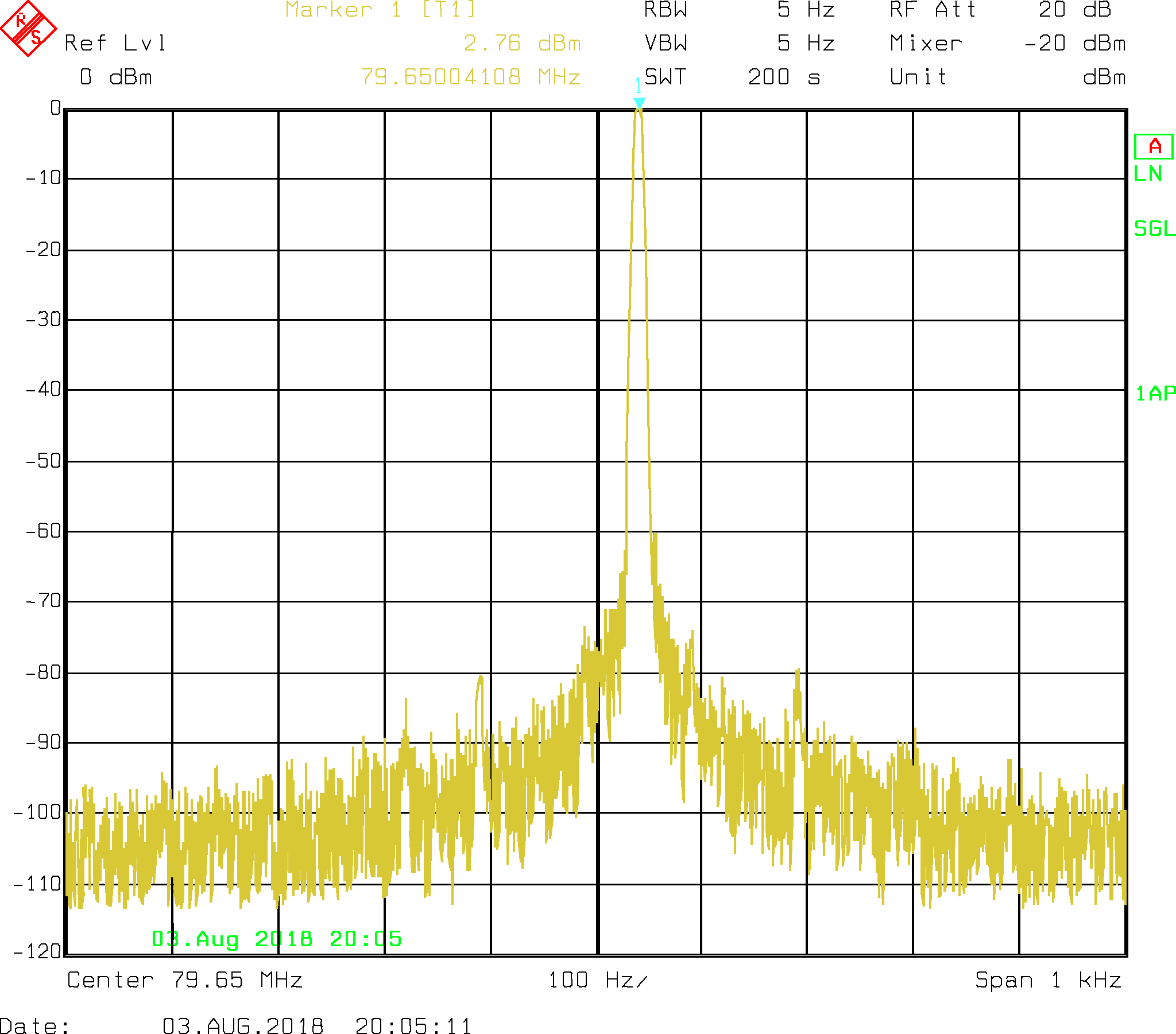 . In the time domain the LVDS signal of LO1 looks like this
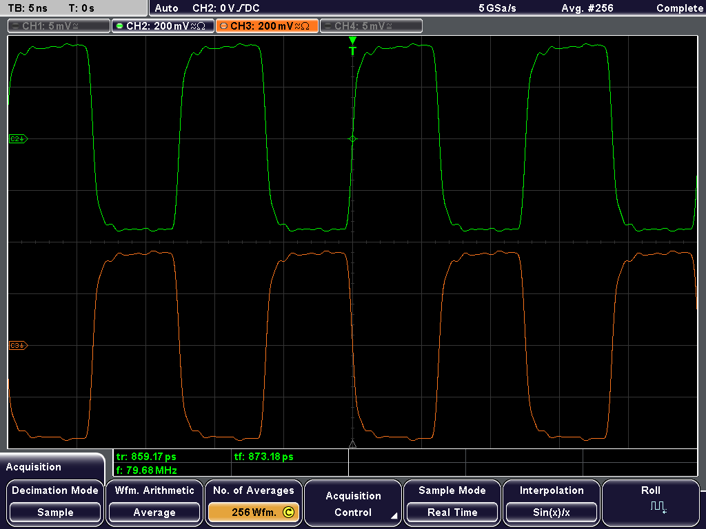 . The settling time after frequency changes is very fast with no appreciable glitches even when the receiver is tuned very fast.
As already mentioned, the LO1 signal is transmitted in LVDS format to the A1 board via two 50 Ohms coaxial cables. The LO2 and BFO signals as well as the LO3 signal for conversion to the third IF of 455 kHz in FM mode are generated as single ended LVCMOS signals by A2-U4, and are transmitted through three line buffer amplifiers to A1; these also set the required signal levels.
The time base for the PLL chip is a very precise TCXO A2-U2, manufactured by Connor Winfield, which is working at 40 MHz and has 0.28 ppm stability over the commercial temperature range from −40°C to +85°C.
As has been learned the hard way when designing the first version of this receiver, the layout and blocking of supply voltages for the individual outputs of A2-U4 are very critical in order to avoid crosstalk between the outputs. A four layer board with continuous ground plane is mandatory here.

A3 Front panel board
This is the front panel board with LED displays and pushbuttons with status LED indicators. This board also passes the signal from the rotary encoder on to A2.
The rotary encoder is an optical one manufactured by Bourns (model ENA1J-B28-00128L), which has 128 steps per revolution, and is fitted with a solid machined and anodized aluminium knob. Neither the encoder nor the knob are cheap, but they allow for very smooth and comfortable tuning.


A4 Power supply board
This board contains two mains transformers (two transformers because no suitable toroidal module transformer with three secondary windings seems to be available, and having a toroidal module transformer custom manufactured was deemed uneconomical) and a pretty standard linear power supply to power three voltage rails: +5 V digital, +5 V analog, and −5 V analog. There is one 2.5 V bandgap reference (A4-U3) which supplies the reference voltage for the +5 V analog rail; all other rails are referenced to that rail. There is an overcurrent protection and a crowbar circuit for each rail. The pass transistors are protected by a thermal cutout.
Note that on the A2 board there are two further linear regulators which generate +3.3 V and +1.8 V to power the PLL chip A2-U4.


A5 Preselector board
This board contains a simple 6-octave-band preselector, the bands are noted on the schematic as well as in the following:
- Band 1: 0 ... 1.5 MHz
- Band 2: 1.5 ... 3 MHz
- Band 3: 3 ... 6 MHz
- Band 4: 6 ... 12 MHz
- Band 5: 12 ... 24 MHz
- Band 6: 24 ... 32 MHz
The five bandpass and one lowpass filters are switched into the signal path by telecom signal relays. There is also a bypass path to disable the preselector. As can be seen from the picture and the board layout files, the filters are realized by good but standard SMD inductors. Of course this puts limits on the linearity of the preselector, but it still may be of value in difficult receiving situations. The entire A5 board is mounted in a die cast aluminium box for shielding. The box is Hammond model 1590N1FL, it has flanges for panel mounting. The board is mounted on hex standoffs, and is designed in such a way that it can be merged into the enclosure with the angled SMA jacks in place.

Some design considerations
As is to be expected, grounding and shielding is critical in such a device, especially with the open board layouts, and all analog signal processing on a single board. For this reason the A1 and A2 boards have four layers, each with a solid ground plane. A low impedance ground connection is provided by the mounting standoffs and the aluminium panel to which they are bolted.
Critical circuits have been placed under board level shields with removable covers manufactured by Laird Technologies, which have sometimes been subdivided in individual compartments. To obtain a dividing wall, a board shield has been cut apart and its side wall has been soldered in place as a divider. In particular, the numerous signal transformers are susceptible to electromagnetic interference, and their placement is important. For this reason I have spent a lot of time to work out an optimal placement of the individual sub-circuits on the A1 board. The board level shields are okay but of course cannot keep up with a solid milled aluminium shield. Moreover, local filtering of supply voltages and control signals is essential, and a large number of capacitors, inductors and ferrite beads are employed for this purpose.
All in all the blocking and shielding concept is quite effective, albeit not perfect. There is a small amount of coupling of the second harmonic of the first IF frequency into the frontend. This is caused by the limiter A1-U11, as can be easily determined by using near field probes. Moreover, there are two or three small spurious tones near the noise floor, but given the simple and compact mechanical construction one can be satisfied with the receiver's spurious content.
Performance
Some performance test results are reported in this pdf file. If time permits I will describe the test procedures in detail, however, for now I can only report some results.
The antenna input referred third order intercept point (TOI) has been determined to be in excess of 30 dBm in a two-tone measurement with the tones spaced at 50 kHz. Large TOI levels are not easy to measure as it is difficult to combine two signal generator outputs in a linear and intermodulation free manner. More exacting measurements which do not merely give a lower bound would increase the expenditure considerably. The sensitivity of the receiver is good, but not stellar, as was to be expected in view of the passive first mixer, and with the first gain stage following the roofing filter. To amend this situation I had included the preamplifier in the design. However, with a sensitivity of about −110 dBm for AM at 2.4 kHz bandwidth the receiver is sufficiently well equipped, and in almost all receiving situations the external noise will be well above the sensitivity level.
One interesting parameter is the antenna input return loss since it indicates the precision of the frontend design. It has been measured to be less than about 10 dB with attenuator, preselector and preamp out, the results can be seen here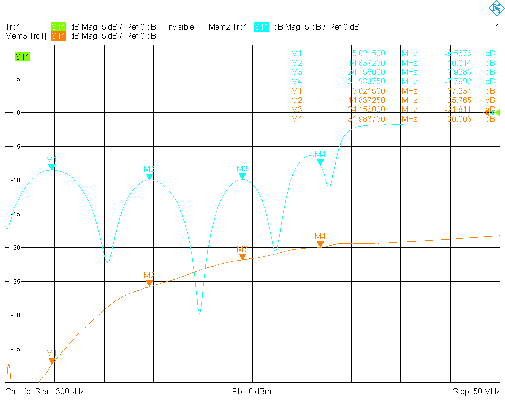 , the blue curve is the return loss with attenuator out, the red one with attenuator in. Even though the result is satisfactory for a communications receiver, the ripple shows that there is room for improvement.
Possible improvements and open problems
After completing such a device and measuring its performance one naturally observes a few opportunities for possible improvement, even though this is the second version of the same basic design. The following lists a few of these, although the list is certainly not complete.
- The AGC in fast mode is on the verge of instability, and sometimes even a little bit beyond. One should decrease the P-gain of the AGC controller (A1-R157).
- The preamplifier, as already mentioned.
- The sound quality of the small internal speaker is not very good.
- There is a lot of room to improve the firmware:
-
- A calibration routine could be added to correct the RSSI readout depending on frequency and level, as well as on attenuator and preamplifier setting. The calibration values could be stored in the internal EEPROM of the microcontroller, and be modifiable by a front panel procedure.
- A similar calibration routine could be implemented to correct for frequency deviations of the TCXO time base.
- Due to the operational principle of the SSB demodulator, the zero beat frequency is in the center of the IF filter. Therefore, in practice one would shift it by entering an appropriate BFO offset, and would mentally add or subtract this value from the frequency display. Of course, this could be automated in software.
All in all this receiver is not perfect, but a considerable improvement over its predecessor. It is quite usable in practice and performs well.