Another RF signal generator based on the LMX2582 and a DDS synthesizer
After building two single-board RF signal generators, one based on the ADF4351 single-chip PLL synthesizer with integrated wideband VCO and output dividers from Analog Devices, and another one based on the competing LMX2582 by Texas Instruments, which has somewhat better specifications and allows higher PFD frequencies, I built yet another one, designated appropriately as the Mk III Signal Generator.
The goal was to try a different concept with the LMX2582: In this circuit, its PLL is run in integer-N mode only, as this avoids integer boundary spurs in the output signal. A fine frequency resolution is achieved by feeding its reference input from a DDS synthesizer. This comes at the cost of somewhat higher carrier phase noise, partly because a cheap AD9951 integrated DDS synthesizer is used. There are some other improvements over the predecessor like a more powerful microcontroller, which allows more comprehensive software calibration facilities and a frequency sweep functionality. Also, there are number of improvements in circuit and firmware details. However, the overall concept remains simplistic; the design still only uses a single standard FR4 board, yet it features an accurately leveled output from about −40 dBm to +10 dBm over a frequency range of 1 MHz to 4.2 GHz.
Since the design is very much derived from the two predecessors, there are many similarities. Therefore the following description closely parallels the previous ones, with changes in the appropriate places.
This project has been delayed for a long time due to the global component shortage in the years 2021–2023, during which a number of key components were unavailable on the market. This was the case for the Texas Instruments LMX2582 and the ATSAM-E54 microcontroller from Microchip Technology, among others.
Mechanical construction
The signal generator is built on a single four layer board with the dimensions 160×160 mm. The board is lightly populated to facilitate easy manual assembly and soldering. It is housed in a Hammond model 1455 R 1601 extruded aluminium enclosure.


The front and rear panels have been manufactured by Schaeffer AG from Berlin, using their software “Frontplatten-Designer”. The board was designed with KiCad version 7.0.6 and manufactured by JLCPCB with their impedance controlled process using prepreg type 7628. The microstrip features in the board layout assume the the following data:
- Prepreg thickness: 0.2 mm
- Prepreg dielectric constant: 4.60
- Outer layer copper thickness: 35 μm
According to the standard approximation formulas this leads to a 50 Ω microstrip trace width of about 0.349 mm. The top layer of the board is used for RF signals, whereas the bottom layer contains all non-RF control signals; the first inner layer from top is a solid ground plane, the second inner layer is used for power.
Circuit diagram and design data
The schematic of the signal generator consists of nine pages and can be viewed here as a pdf file. The complete design data including KiCad schematic and board files, Gerber files, the firmware source code (written in C), the front and rear panel artwork and the GNU Octave scripts for automatic calibration, is included in this zip archive. Hopefully, the source code is sufficiently commented to be comprehensible.
Circuit description
Just like the previous versions the signal generator uses a “headless” design without front panel controls. The generator is a self-powered USB 2.0 device of class CDC, and establishes a virtual COM port on the host PC. For basic control a simple terminal program is enough, even though this is not very convenient. It would be better to create some software with a graphical user interface, even though I have not gone to this effort. The USB port is handled by the main microcontroller U26, a Microchip (Atmel) ATSAME54P20A, which also controls all other devices on the board, either via SPI or directly through GPIO lines. This microcontroller contains a 32-bit ARM Cortex M4F CPU with internal FPU, and runs at 100 MHz in this application. The CPU clock is derived from the internal TCXO reference U1. The application code uses FreeRTOS and some Microchip drivers and middleware. The firmware can be downloaded to flash memory though the 10-pin 50 mil ARM Cortex SWD debug header which is available on the board.
All calibration data and up to 100 instrument setups are stored in the 256 Kbit serial EEPROM U27. The calibration data is checksum protected and loaded into SRAM at startup; default values are loaded when the calibration data is found to be invalid. Microcontroller U26 is connected to two general purpose debug LEDs on the main board, which can be useful for firmware development. There are three further LEDs which indicate lock of the main and reference PLLs as well an output unleveled condition. A single front panel status LED is provided; it lights green during normal operation, and red when an error occurs (e.g. a loss of lock of one of the PLLs, the output being unleveled, an argument of a received command being out of range, or invalid calibration data in EEPROM, etc.). Moreover, for development purposes an on-board reset pushbutton SW1 for microcontroller U26 is provided.
Frequency processing starts from the internal reference U1, a 10 MHz TCXO made by Connor-Winfield. The part No. DV75D TCXO fitted in my prototype is not really up to the task (stability ±1 ppm) and should be replaced, e.g., by Connor-Winfield part No. DV75C with ±280 ppb stability and better phase noise specification. That part has the same footprint. Next, the ultra-low phase noise VCXO U6, running at 100 MHz, is phase locked to the reference frequency by means of integer-N PLL U5, an ADF4002 from Analog Devices, containing RF and reference frequency dividers, a phase-frequency detector (PFD), a charge pump, and lock detect circuitry. The VCXO is a CVHD-950X-100.00 by Crystek; it features a HCMOS output and a phase noise floor of about −166 dBc/Hz. Resistors R18, R19, and R20 set the appropriate signal levels. Low-noise voltage regulator U4 powers the VCXO. The loop bandwidth of the reference PLL is adjusted to about 50 Hz with 50 degrees of phase margin by the three-pole loop filter C29, C30, R16, R17, C33 and C35. In this way the low phase noise of the VCXO is not much impaired by the reference, even close to the carrier. Provision is made to connect an external reference frequency. The external reference signal is conditioned by U2, a TLV3501 high-speed comparator from Texas Instruments, and is routed to the reference input of U5 when commanded by microcontroller U26. Resistor R3 and diodes D2 and D3 protect the external reference input.
The phase locked 100 MHz signal from VCXO U6 is passed on to DDS synthesizer U8, an AD9951 from Analog Devices. It contains a 14-bit DAC with current sink outputs and a DDS core with a 32-bit tuning word. Its analog supply voltage (feeding the DAC) is provided by low-noise voltage regulator U7. The 100 MHz signal is quadrupled by the internal PLL in U8, so that the DDS core is clocked at 400 MHz. The DAC current sink outputs are converted to a 50 Ω voltage source by means of balun T1 and resistors R27 and R29. The DAC reconstruction filter is a steep three-trap elliptic filter with 120 MHz cutoff frequency, 0.8 dB ripple, and 85 dB calculated attenuation. In the range from 1 MHz to 20 MHz the DDS is directly used to generate the output signal. For that purpose it is buffered by amplifier U9, which is set up for 6 dB of gain, and is fitted with an additional low-pass filter L5–L7 and C81 at the output. Amplifier U9 is deactivated by means of Q2 when not in use at output frequencies above 20 MHz. For output frequencies from 20 MHz to 4.2 GHz the DDS provides the reference frequency for the main PLL synthesizer U11. Then its output is 100 MHz or slightly less in order to achieve a fine frequency resolution, since the main PLL only runs in integer-N mode.
At output frequencies between 20 MHz and 4.2 GHz the output signal is generated by U11, which is a LMX2582 wideband PLL frequency synthesizer with integrated VCO by Texas Instruments. Its reference frequency from the DDS U8 is converted to differential by the 2:1 balun T2, and is then directly fed into the phase-frequency detector (PFD); all internal reference dividers and doublers are disabled by the firmware for best phase noise performance. Also, in this way the PFD frequency is kept below 100 MHz in order to limit the level of PFD-related spurs in the output signal. The VCO of U11, which really is a set of separate VCOs with several bands, operates between 3.55 GHz and 7.1 GHz, and requires a calibration procedure each time the frequency is changed. The firmware in U26 will trigger this calibration procedure upon frequency changes. To achieve a clean output signal and to isolate the internal VCO from the charge pump as much as possible, it is powered from low noise voltage regulator U10; also all other power rails have a good amount of filtering and decoupling. I've found that the internal VCO can become unstable towards the lower end of its operating range at 3.55 GHz, and is best run at 3.6 GHz or higher (the firmware takes care of this observation).
The maximum output frequency of U11 is 5.5 GHz, although it is only used up to 4.2 GHz in this application in order to limit the number of necessary harmonic filters. Also, the design of wider bandwidth output and leveling circuitry would become more difficult, especially on a simple FR4 board. Below output frequencies of 3.6 GHz, the minimum VCO frequency, several channel dividers in U11 must be switched into the signal path. There is one divider which can either divide by 2 or 3, and two dividers which can divide by 2, 4, 6 or 8. The dividers can be combined by means of a multiplexer. For a specified output frequency, microcontroller U26 takes care of the proper setting of the dividers and the multiplexer, and keeps the VCO frequency in the allowable range and as small as possible to optimize phase noise.
Since the DDS core of U8 is clocked at 400 MHz and features a 32-bit tuning word, the minimum frequency step around 4.2 GHz (leading to an PLL integer divider of $N=42$, including a factor of $2$ due to the prescaler) is \begin{align} \Delta f&=\Delta f_{\rm pfd}\cdot\text{prescaler}\cdot N\cdot\frac{1}{\text{channel divider}}\\ &=\frac{\text{DDS sysclk}}{2^{32}}\cdot\text{prescaler}\cdot N\cdot\frac{1}{\text{channel divider}}\\ &=\frac{400\,{\rm MHz}}{2^{32}}\cdot42\\ &\approx3.91\,{\rm Hz}. \end{align} The minimum frequency step around 1 GHz is about 0.93 Hz, which is below the setting resolution of 1 Hz. Due to the frequency processing, “round” output frequencies like 1 GHz, 100 MHz, and many more, are reproduced exactly.
The output of U11 is converted from differential to single ended by T3, a wideband 2:1 transmission line type balun from Mini-Circuits, which also achieves some gain (3 dB in theory, disregarding its insertion loss). A GaAs SPDT switch U12 (part No. MASW-008853 from M/A-COM) changes between the DDS and PLL synthesizer beyond output frequencies of 20 MHz; below 20 MHz the output stages of U11 are deactivated to help prevent spurs in the output signal. This switch is followed by the voltage variable attenuator U14, which is part No. HMC346AMS8GE by Analog Devices (a former Hittite part), and which is controlled by op amp U13. This voltage variable attenuator is part of the automatic level control loop.
The voltage variable attenuator is followed by a 9-band harmonic filter bank. The individual low-pass filters are switched by U15 and U18, two HMC321ALP4E GaAs SP8T RF switches by Analog Devices (formerly a Hittite part). Since there are altogether nine filter bands, the lowest two bands are further multiplexed by two MASW-007221 SPDT GaAs switches U16 and U17 from M/A-COM. All switching is done automatically by microcontroller U26, depending on the required output frequency. The following table lists the corner frequency and frequency range of use for each filter:
| Band | Corner freq. (MHz) | Output range (MHz) |
|---|---|---|
| 1 | 39 | 20 … 36 |
| 2 | 69 | 36 … 65 |
| 3 | 124 | 65 … 117 |
| 4 | 220 | 117 … 211 |
| 5 | 400 | 211 … 380 |
| 6 | 720 | 380 … 685 |
| 7 | 1300 | 685 … 1230 |
| 8 | 2340 | 1230 … 2215 |
| 9 | 4200 | 2215 … 4200 |
The filters of band 1 to 7 are realized as lumped component LC filters. After designing them they have been built on a test board and measured with a network analyzer. The filters of band 8 and 9 are realized as microstrip stepped impedance filters; they have been tested in an EM simulation (using QucsStudio with openEMS) and also been measured with a network analyzer. There is good agreement between simulation (band 8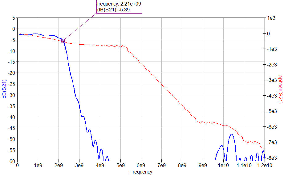 and band 9
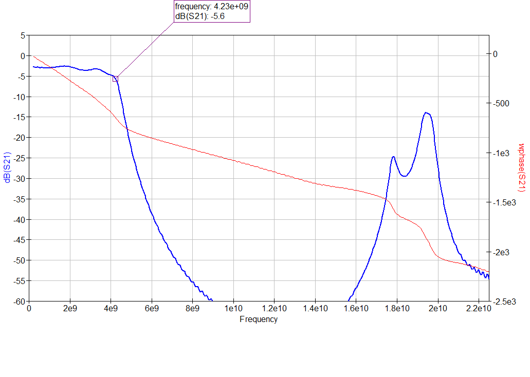 ) and measurement (band 8
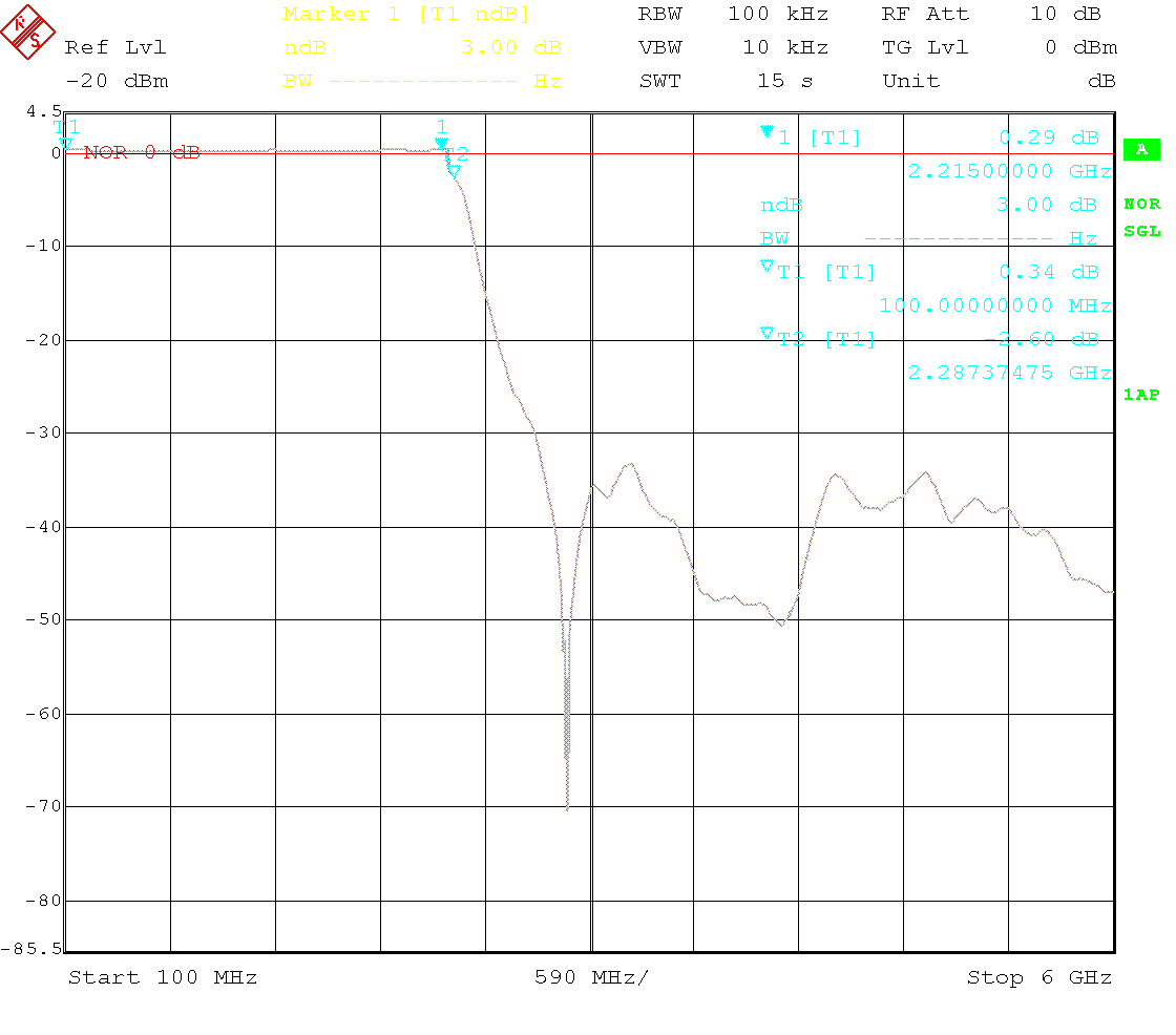 and band 9
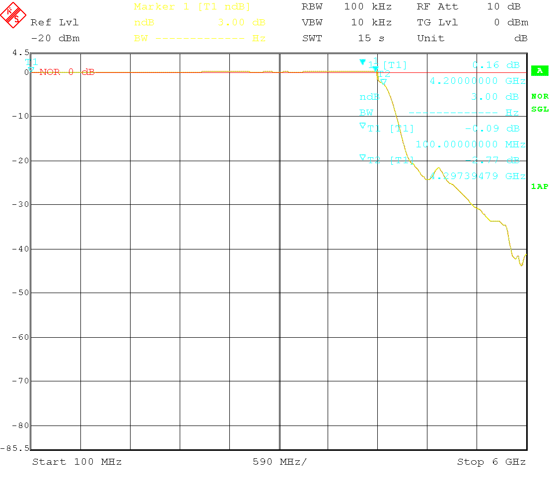 ).
).
The filter bank is followed by U19, a GVA-63+ InGaP HBT MMIC amplifier from Mini-Circuits. At its output follows the resistive signal tap T4, a model RBDC-20-63+ from Mini-Circuits, with very low insertion loss and a coupling ratio of about 20 dB. It taps off a sample of the signal after U19, which is further attenuated by 10 dB by means of MMIC attenuator U20 (HMC656LP2E by Analog Devices) for use by the level detector U21, an AD8319 by Analog Devices. This level detector is part of the automatic level control (ALC) loop. After T4, the RF resistor R59 sets the output impedance to 50 Ω.
The ALC loop is closed within level detector U21, which compares the detected voltage, proportional to the signal level after U19, with the level setting voltage at pin 7 of U21, which is supplied by a 12-bit DAC U25. It is referenced to U28, a REF3425 voltage reference with 6 ppm/°C, which ensures adequate level stability over temperature. Between the output of U21 and the voltage variable attenuator U14 is a low-noise rail-to-rail op amp U22, which shifts the output voltage to the range from −5 V to 0 V to satisfy the biasing requirements of U14, and also sets the ALC bandwidth to approximately 16 kHz. Comparators U22 detect if the output signal is unleveled; this condition is monitored by microcontroller U26.
After the signal tap T4 follows gain equilibrator T5, which is model EQY-10-63+ by Mini-Circuits, and then an InGaP HBT MMIC amplifier U23, a GVA-84+ by Mini-Circuits, with about 24 dB of gain and a 1 dB output-referred compression point of about 20 dBm. The purpose of the gain equilibrator is to approximately compensate the roll-off of U23 since it is not within the ALC loop. The reason for placing the signal tap between amplifiers U19 and U23, and hence having U23 outside the control loop, is that a loss of 6 dB plus the insertion loss of T4 (about 1 dB) is incurred over T4 and R59. Hence there would not be enough headroom left to drive the output to 10 dBm without adding a too large amount of harmonics.
Finally, U23 is followed by the digitally controllable GaAs MMIC step attenuator U25, which is a HMC629ALP4E by Analog Devices (a former Hittite part). This attenuator can be set between 0 dB and 45 dB in steps of 3 dB, and has an insertion loss of a little less than 3 dB. It is used for coarse level setting, and is under automatic control of microcontroller U26. Fine control of the output level is done by DAC U29. Frequency dependent level correction by means of a calibration table stored in EEPROM U27 is performed automatically.
The generator is operated from a DC voltage of approximately 3.3 V to 12 V, supplied to a rear panel barrel jack. The power supply consists of buck/boost converter U30, a LTC3119 by Analog Devices (formerly a Linear Technology part), which runs at a switching frequency of a little less than 1 MHz and outputs stable 6 V. This voltage is filtered and passed on to two low dropout linear post regulators U31 and U34, which generate clean 5 V and 3.3 V for noise critical analog circuitry. Another linear regulator, U33, generates 3.3 V for digital circuitry, with less filtering. Noise critical components such as VCXO U6 and the internal VCO of U11, have their own local low-noise linear regulators, which are LT3042 by Analog Devices (a former Linear Technology part). Another switchmode converter U32 with Ćuk topology, a LT3462 by Analog Devices (also a former Linear Technology part) generates −5 V to bias the voltage variable attenuator U14. This power rail must also be well filtered. The power input is filtered to prevent switching noise from leaking into the power cable.
Power consumption is about 6 W, depending on input voltage (U30 becomes less efficient for input voltages below 5 V). At 5 V the current consumption is around 1.2 A, depending on output frequency.
Operation
As was explained above, the signal generator is operated via a USB CDC interface, which establishes a virtual COM port. This pdf document briefly describes the protocol for controlling the generator.
Calibration
The calibration values for correcting the internal frequency reference, the output level and attenuator stages, and the slope of level detector U21, are stored in EEPROM U27. This EEPROM also stores up to 100 instrument setups. The firmware is parametrized for calibration points with 5 MHz spacing between 1 MHz and 100 MHz, and with 100 MHz spacing between 100 MHz and 4.2 GHz. At each of these frequency points, there is one calibration value which sets the overall flatness of the signal path, and one for each attenuator stage (3 dB, 6 dB, 12 dB and 24 dB). The attenuator correction values are added depending on which attenuator stages are engaged. Between two frequency points, linear interpolation is performed for both the overall signal path correction as well as for the attenuator correction.
In theory, all calibration values could be determined by hand, using a power meter and a frequency counter. However, this would be extremely tedious. Therefore, I wrote a script in GNU Octave which completely automates the calibration of the unit (see the zip archive linked above for the script). The script assumes a Rohde & Schwarz NRVD power meter with an appropriate power sensor (I have used a Rohde & Schwarz NRV-Z1 diode power sensor). The power meter is assumed to be controlled by a Prologix GPIB adapter. The script could, however, be easily modified to accommodate other power meters. It also uses the digital frequency correction feature of the Rohde & Schwarz power sensors by setting the NRVD to the appropriate frequency in order to apply the correction. The script will also prompt the user to connect the power sensor or the frequency counter as required, and it checks whether the required tolerances were achieved.
Performance
Spectral purity near the carrier
We start by taking a close look at the spectrum in the vicinity of the carrier. The results for carrier frequencies of 10 MHz, 100 MHz, 1 GHz, 2 GHz, 3 GHz and 4 GHz, and at an output level of −10 dBm, are shown in the following pictures. All spectra have been measured with 100 Hz resolution bandwidth and 20 Hz video bandwidth, and with the auto peak detector. In all of the following measurements, the signal generator was run from a stable and very clean external reference.


It can be seen that the close-in phase noise is somewhat higher than with the previous version where the LMX2582 was directly run from a very clean VCXO with 100 MHz PFD frequency. This is to be expected because the DDS output signal is noisier than a good VCXO. However, the advantage of this approach is the absence of any integer boundary spurs.
Harmonics and spurs
Next we look at the harmonic and spurious content of the output signal for various carrier frequencies. Also, the spectra in the following pictures indicate the performance of the harmonic filters.


For example, one reads off a harmonic suppression of about 48 dB of the first harmonic for a 1 GHz carrier. Checking some other carrier frequencies shows that a harmonic suppression of at least 30 dB is achieved consistently, and often much better, which is a satisfactory performance. On an oscilloscope, the output signal therefore appears as a perfect sine wave, as can be seen here at 50 MHz and +10 dBm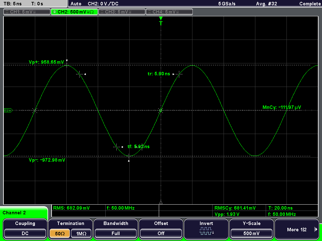 with a scope bandwidth of 500 MHz.
Notice the subharmonic at an output frequency of 4 GHz and at −27 dBc. It appears at output frequencies greater than 3.6 GHz when the LMX2582 is running without a channel divider, and the VCO is routed directly to the RF output.
At higher output frequencies, there are some low level spurs visible, spaced 100 MHz apart. These are due to the PFD or the charge pump. They are at higher levels than the specification in the datasheet (less than −93 dBc at a PFD frequency of 20 MHz). The higher spur levels are due to the higher PFD frequency of 100 MHz used in this application, and possibly to some extent due to a coupling mechanism outside the chip. These spurs are a general problem with integrated synthesizer chips like the LMX2582 because of the close proximity between VCO and charge pump, and cannot be fully avoided when high PFD frequencies are used, which, on the other hand, is desirable to achieve a good phase noise performance.
Output leveling
Output level accuracy is determined by the level correction values stored in EEPROM U27. One could increase the density of the calibration points by changing some parameters in the source code, the EEPROM size still allows for a larger number. Level accuracy was measured with a power meter and a power sensor (the same power sensor that was used for calibration).

It can be seen that for levels below −40 dBm and frequencies greater than 2 GHz the traces show some instability. This is likely due to the chosen method of calibrating the attenuator stages individually and adding their correction values, depending on which attenuator stages are engaged. While this may be appropriate for a mechanical attenuator, it might be worthwhile to experiment with another method for this MMIC attenuator. For example, one could record correction values for different level settings at each frequency point (say, 5 dB apart) and interpolate between them. Also, a proper shielding of this circuit section (like a milled enclosure with an individual chamber for the attenuator chip) might help.
The maximum output level obtainable when setting the generator to +10 dBm can also be seen in the previous picture. From 3.5 GHz onward the output amplifiers are not able to maintain the maximum settable level of +10 dBm, and the generator shows an ALC unleveled error. A level of 0 dBm is achieved at all frequencies though.
Settling time
The settling time after frequency or level changes depends on the magnitude of the frequency or level change. The picture below shows an example of a frequency change from 100 MHz to 1 GHz.

The measurement shows a settling time of about 211 μs, mainly due to the ALC bandwidth. The LMX2582 has some facilities which enable a fast lock of its PLL. Some of these have been enabled in this design (see the datasheet and the source code).
Residual AM and FM
The residual AM and and FM of the carrier was also measured, with the generator locked to an external stable 10 MHz reference. At carrier frequencies of 1 GHz and 4 GHz a residual FM of less than 13.6 Hz and 49.3 Hz RMS, respectively, was measured over a bandwidth of 20 kHz. Residual AM was measured to be less than 0.1 % RMS over the same bandwidth at both carrier frequencies. These are satisfactory results, although they are, unsurprisingly, somewhat higher than with the previous version.


Conclusion and possible improvements
Compared to the previous version, this generator performs better due to many improvements in various details. The close-in carrier phase noise is, however, somewhat higher. This was expected since the main PLL is running from a DDS, which is noisier than a very low noise phase locked VCXO.
As was mentioned above, it might be worthwhile to experiment with different attenuator calibration methods. Also, the settling time could still be improved to reduce glitches, especially during fast sweeps.
Nevertheless, in spite of the very simple design, the generator performs satisfactorily, and is quite usable in practice. This version seems to be close to what can be achieved with a simple design like this. Further improvements like a cleaner output signal (less PFD spurs and lower phase noise) would require more drastic changes like separating the VCO from the charge pump, i.e., abandoning the use of an integrated RF synthesizer chip like the LMX2582, and using a cleaner (and much more expensive DDS synthesizer). Also, a proper shielding would help to reduce spurs and increase level accuracy.
Addendum
When readers of this site replicated the device, the following problem arose: After calibrating the signal generator, it turned out that the setting range of the voltage variable attenuator U14 is insufficient: For some output level settings and at some frequencies below 1 GHz the device indicates an “ALC unleveled” error, with the attenuator at maximum attenuation. This could be fixed by changing a parameter in the firmware. In the version offered above for download (which works well in my copy of the generator), the output level of the PLL frequency synthesizer U11 is reduced below output frequencies of 100 MHz. Changing this switching point to 1.2 GHz solved the problem (change line 126 in file app_instr_state.h to #define FREQ_DRV_LVL_CHANGE 1200000000UL).