A GNSS Time and frequency receiver
There are a number of GPS disciplined oscillator (GPSDO) projects and circuits online, yet I decided to develop my own in order to implement some special features and to make a few improvements. The least important difference is that I call it GNSSDO or GNSS Time and Frequency Receiver (with GNSS standing for Global Navigational Satellite System) on the front panel and in the firmware since it does not only receive the satellites of the NAVSTAR GPS system run by the US Armed Forces.
Like most GPSDOs this device disciplines an OCXO in order to provide a stable and accurate reference frequency (10 MHz), but it also supplies a pulse-per-second (PPS) signal aligned with the GNSS time scale (pulse at top of the second) which is derived from the internal 10 MHz OXCO. Hence the somewhat pretentious name “time and frequency receiver” (because the UTC at the last PPS pulse can be queried over the PC interface).
The unit features three separate 50 Ω pure sine wave 10 MHz outputs and a 5 V TTL compatible PPS output, also with 50 Ω source impedance. It can be used with a standard inexpensive active GPS antenna (a supply voltage of 3.3 V is provided at the antenna input).
It is designed to run permanently and autonomously from a power brick, and uses a supply voltage between about 3.3 V and 12 V. Power consumption is dependent on the OCXO; with the Taitien Model NI-10-MHZ-2500 OCXO, it consumes about 4 W when the oven is warmed up. The unit does not have a display, but is equipped with nine status LEDs. USB connectivity is provided, and status information can be queried with a simple terminal program; also configuration can be done this way and stored in a non-volatile memory.
Mechanical construction
The GNSSDO is built on a single four layer board with the dimensions 160×120 mm. Manual assembly and soldering should be easy. The board is housed in a Hammond model 1455 T 1201 extruded aluminium enclosure, but Fischer Elektronik model AKG 165 46 120 ME should also be usable, with slightly modified front and rear panels.
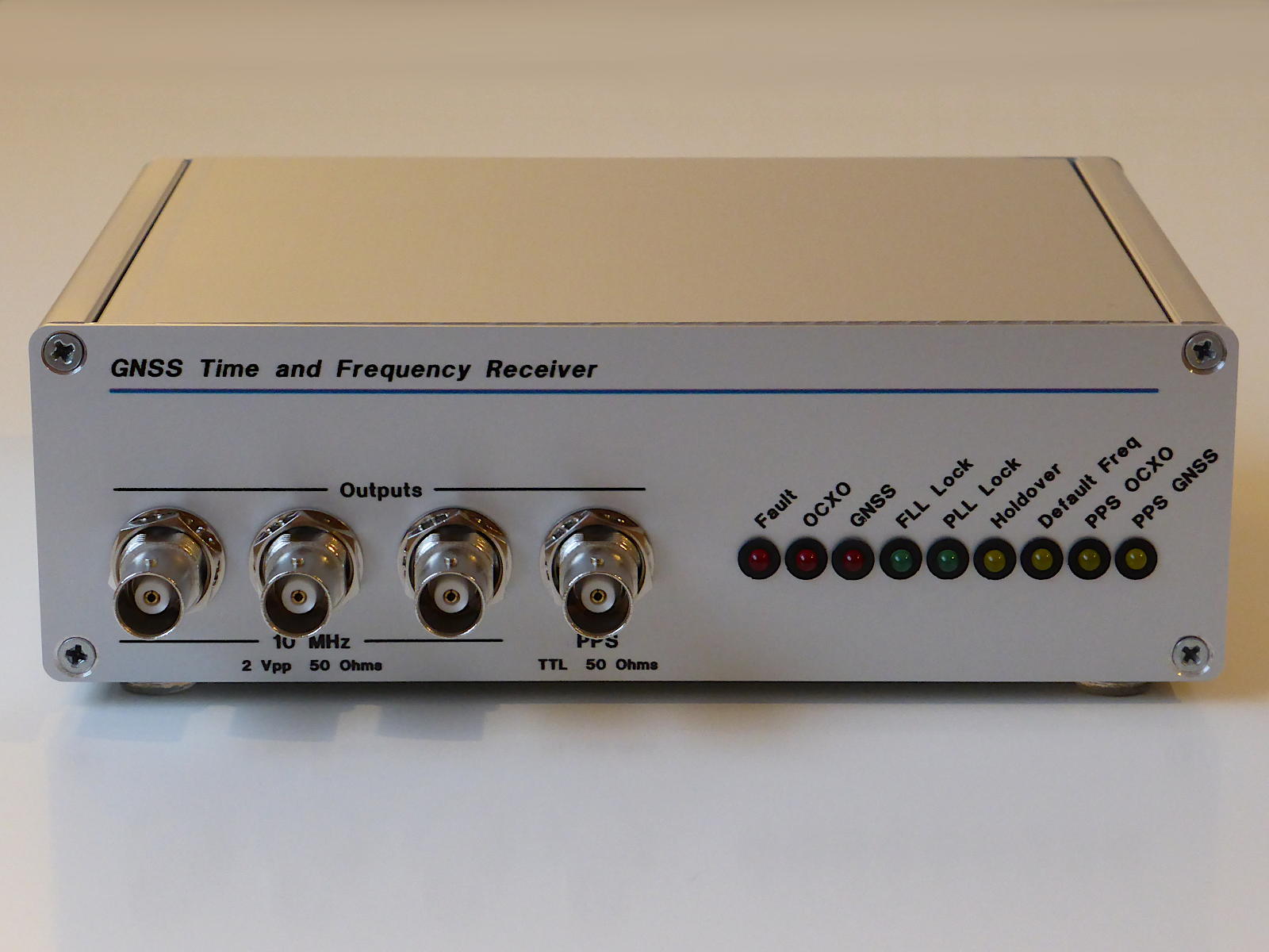

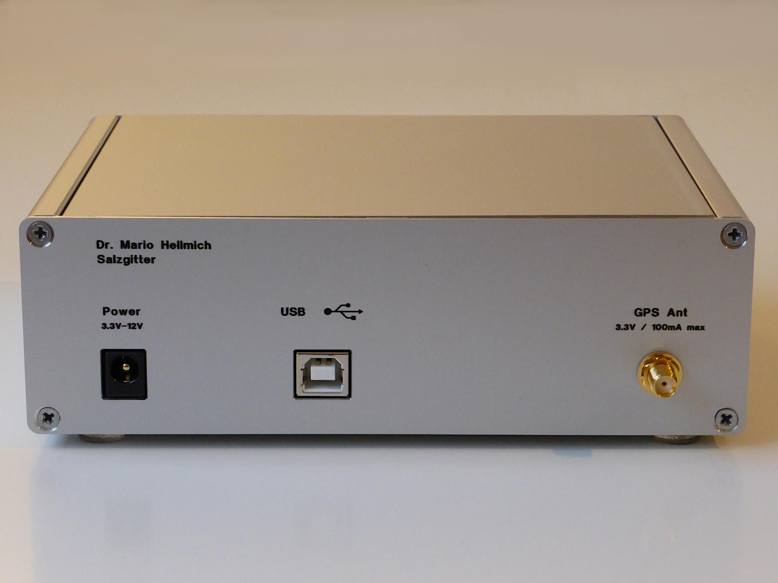

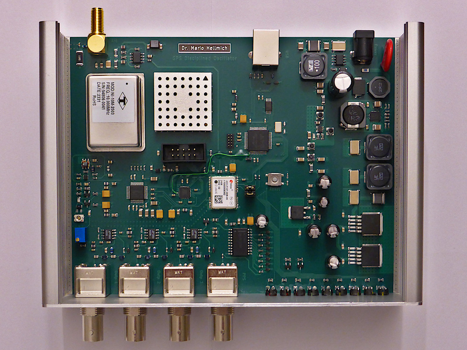

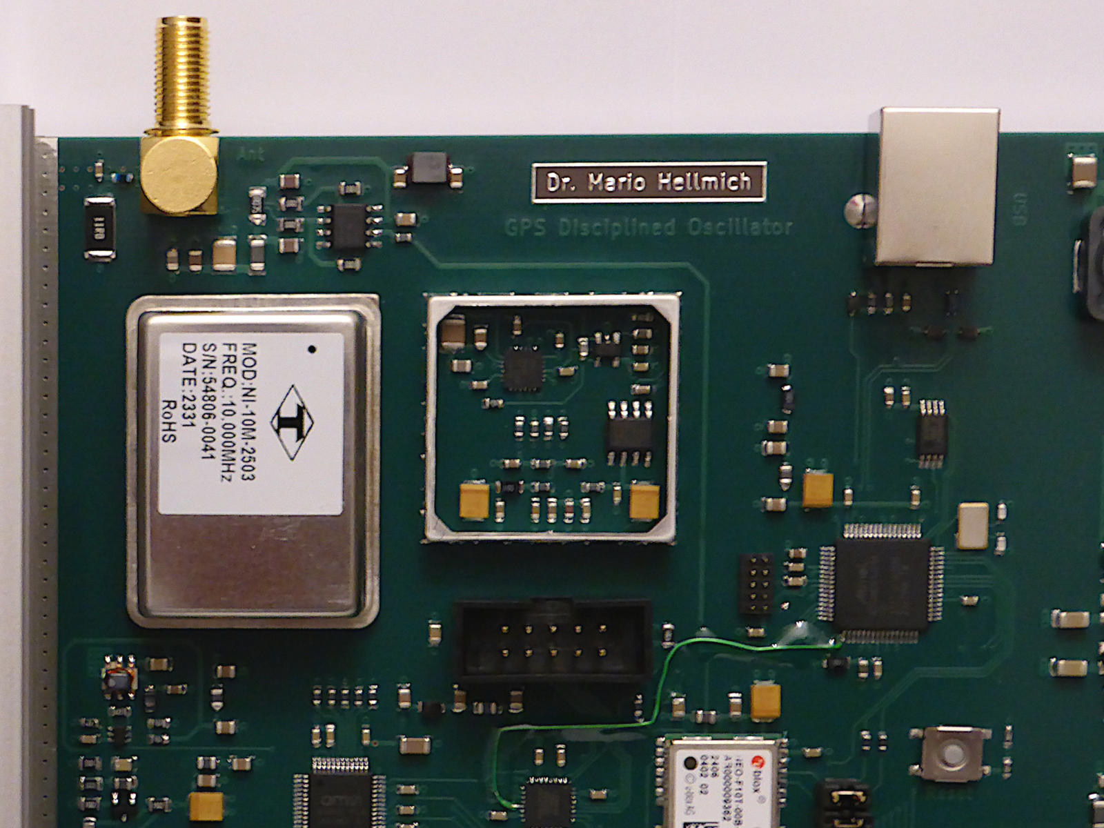

The front and rear panels have been manufactured by Schaeffer AG from Berlin, using their software “Frontplatten-Designer”. The board was designed with KiCad version 8.0.7 and manufactured by JLCPCB with their impedance controlled process using prepreg type 7628. There are no impedance controlled traces except for the GPS antenna connection. Yet the four layer board allows for a continuous ground plane, and hence good EMC properties and a quiet switching power supply design.
Circuit diagram and design data
The schematic of the GNSSDO consists of six pages and can be viewed here as a pdf file. The complete design data including KiCad schematic and board files, Gerber files, the firmware source code written in C (current version: 1.7), the FPGA gate ware (written in Verilog, along with a complete Lattice Diamond project folder, including the necessary constraints and the bitstream files), and the front and rear panel artwork, is contained in this zip archive.
Circuit description
Central to this design is the OCXO U4, which is part no. NI-10-MHZ-2503 manufactured by Taitien Electronics. The footprint fits OCXOs with a CO 08 case according to IEC 60679-3:2012 (Eurocase), such as the Taitien model NI-10-MHZ-3500 double oven OCXO, but these are very pricey when bought new (they are available in very high performance grades). Suitable OCXOs are also available from Kristallverarbeitung Neckarbischofsheim GmbH and Axtal GmbH. The OCXO supply current is monitored by microcontroller U15 via U5, and is used to issue errors such as “OCXO Cold”.
The OCXO EFC (electronic frequency control) voltage is generated by U1, an 18-bit low-noise precision DAC by Texas Instruments, part no. DAC9881. The circuit uses the output amplifier sense feature of this DAC, and the reference voltage is buffered, with Kelvin sense connections for the reference high input. The reference is supplied by U2, a low-noise precision reference from Analog Devices available in temperature coefficients from 0.8 ppm/°C to 4 ppm/°C. Depending on the OCXO tuning range (e.g. 1 ppm) and its temperature coefficient, in most cases a 4 ppm/°C reference will yield a temperature variability well below that of the OCXO itself (also don't forget about the DAC temperature drift of ±0.25 ppm/°C typical).
With the Taitien NI-10-MHZ-2500 OCXO, which has a tuning gain of less than 2 Hz/V, the 18 bits of DAC U1 lead to a frequency variability of about 38 μHz per LSB, which is a relative frequency variability of about 3.8×10⁻¹² per LSB, and should be sufficient to meet a final accuracy of the order of 10-12. The Taitien NI-10-MHZ-3500 has a tuning gain of a bit over 1 Hz/V, yielding a relative frequency variability of 1.9×10⁻¹² per LSB.
The OCXO output signal is converted to 3.3 V LVCMOS by balun T1 and high-speed comparator U6, and no direct use of the OCXO output is being made, therefore the circuit can accommodate sine wave and HCMOS output OCXOs with no change, and is independent of the OCXO output level.
The LVCMOS output signal from the comparator is fed to the clock input of FPGA U7 and also to the output circuits. These consist of a 10 MHz tuned amplifier built around Q3 and Q4, which converts the LVCMOS signal to sine wave and passes it on to the three output amplifiers U10, U11 and U12. These are low-noise, low distortion rail-to-rail output op-amps (part no. LTC6228, which was discontinued just a few weeks ago as I write this). The output amplifiers are followed by ESD protection circuitry and a discrete LC low-pass filter to reduce the harmonic content of the output signal. The nominal output amplitude is 10 dBm into 50 Ω.
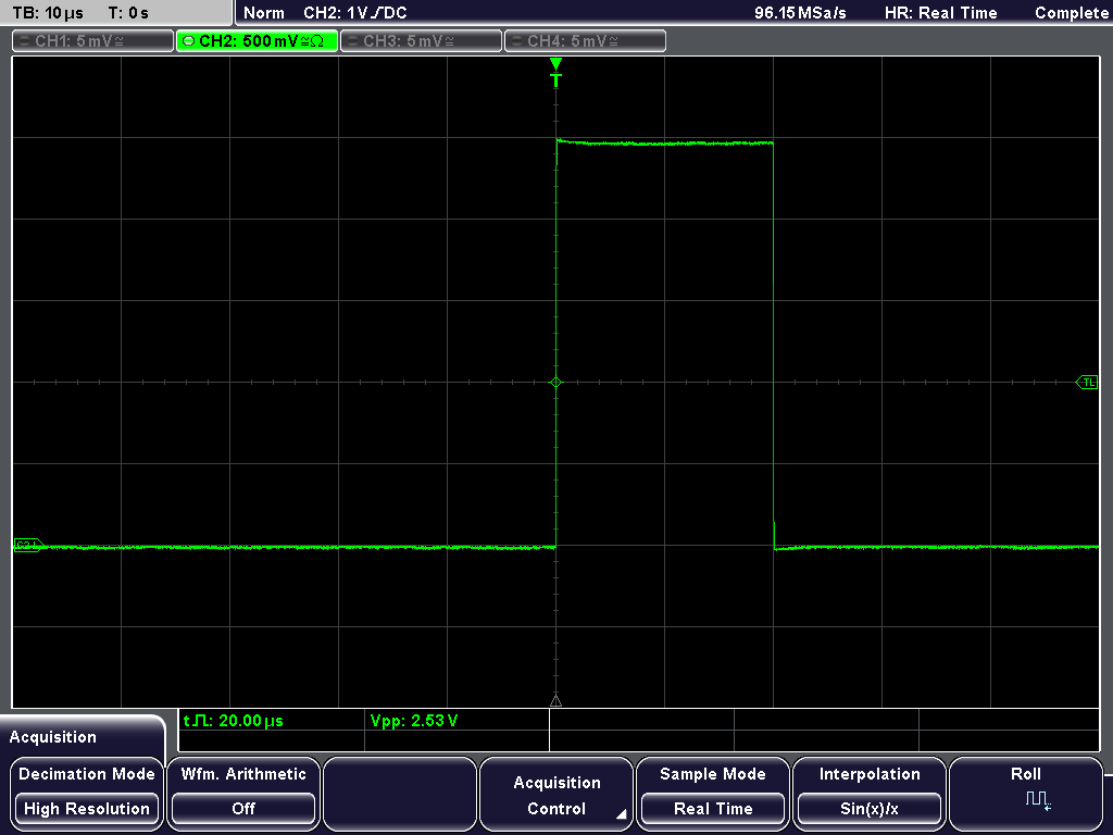
The PPS output signal is generated by FPGA U7 through frequency division of the OXCO output signal, the pulse duration is fixed to 20 μs in the gate ware. The PPS signal is buffered by U9, which is wired up for approx. 50 Ω source impedance. All outputs can be disabled by microcontroller U15 through the Outp-Shdn signal.
The FPGA U7, a small MachXO2 flash FPGA from Lattice Semiconductor, also generates a 5 MHz signal from the OCXO output to clock the TDC U8. Moreover, it generates versions of the PPS signals from the OCXO and from the GNSS receiver U14, each with 10% duty cycle, to drive two front panel indicator LEDs. Also, when commanded by microcontroller U13 though the Sync-Cmd line, it adjusts the phase of the PPS signal generated from the OCXO with that of the GNSS receiver to speed up phase locking.
The time-do-digital converter (TDC) U8, part no. AS6501 by ScioSense, is set up to measure the time difference by the PPS signal generated from the OCXO and that corresponding to the GNSS time scale as supplied by GNSS receiver U14. This chip is not cheap, but provides excellent resolution and temperature stability compared to an analog interpolator circuit. It is clocked with 5 MHz and is configured for a measurement resolution of 2 ps in the firmware. It can measure a maximum time interval of 3.2 s between its two input channels in this configuration before its counter rolls over, and thus can always discern whether the GNSS PPS pulse is early or late relative to the local OCXO PPS pulse. The firmware in microcontroller U15 calculates the phase difference between the two PPS signals and the frequency difference of the OCXO relative to the GNSS time reference, and uses these two data to steer the OCXO through DAC U1.
The integrated GNSS receiver U14 is part no. NEO-F10T by u-blox. It is configured by the firmware in microcontroller U15 at startup or when parameters are changed though the USB data link. Also, timing, navigation and status information is continuously read out by microcontroller U15. It is set up to provide a 1 Hz timepulse signal, which is routed to the TDC U8 and FPGA U7. The timepulse signal has a nominal jitter of ±8 ns (16 ns time mark resolution), but U14 provides correction data (“saw-tooth correction”), which is read out by the firmware and applied to the calculation of phase and frequency deviation.
Microcontroller U13, a Microchip (Atmel) ATSAMD51J20A, controls the circuit and performs the signal processing involved in steering the OCXO. This microcontroller contains a 32-bit ARM Cortex M4F CPU with internal FPU, and runs at 100 MHz in this application (the clock is generated from a separate crystal). The application code uses FreeRTOS and some Microchip drivers and middleware. The firmware can be downloaded to flash memory though the 10-pin 50 mil ARM Cortex SWD debug header mounted on the board. Instrument configuration data is stored in the 256 Kbit serial EEPROM U15, which is read at startup or reset. Checksum test of EEPROM data and wear leveling is provided by the firmware.
Finally, the power supply accepts an input voltage between approximately 3.3 V to 12 V, supplied to a rear panel barrel jack. It consists of buck/boost converter U16, a LTC3119 by Analog Devices, which runs at a switching frequency of a little less than 1 MHz and outputs stable 6 V. This voltage is filtered and passed on to two low dropout linear post regulators U18 and U20, which generate clean 5 V and 3.3 V for noise critical analog circuitry. Another linear regulator, U19, generates 3.3 V for digital circuitry, with less filtering. Switchmode converter U17 with Ćuk topology, a LT3462 by Analog Devices, generates −5 V for the output circuits.
Control loop
The control loop which steers the OCXO is partially realized in software (indicated by dashed boxes in the schematic block diagram). As already mentioned, the TDC measures the time difference between the local OCXO and GNSS PPS signals and the time difference between two successive GNSS PPS signals (using the OCXO as a timebase). From this data microcontroller U15 calculates the phase deviation $\Delta\varphi$ and frequency deviation $\Delta f$ of the OCXO (relative to the GNSS time reference). The loop can use either $\Delta f$ or $\Delta\varphi$ as input, thus implementing a frequency locked loop (FLL) or a phase locked loop (PLL), or it can use a weighted average $\Delta v=\epsilon\Delta\varphi+(1-\epsilon)\Delta f$ of the two, with $0\leq\epsilon\leq1$. When the PLL and FLL are in the locked state (this is continuously checked and indicated by front panel LEDs by a dedicated algorithm implementing a hysteresis, so that short glitches do not lead to a loss of the locked condition—see the code), the weight $\epsilon$ is set to one, and the loop operates as a pure PLL.
In this case the loop contains an implied integrator because of the connection between phase $\varphi$ and frequency $f$, i.e., \[\varphi(t)=2\pi\int_{-\infty}^tf(s)\,\mathord{\rm d}s.\] Therefore, the closed loop transfer function then is \[H(s)=\frac{\mathcal L\varphi_{\rm VCO}(s)}{\mathcal L\varphi_{\rm GNSS}(s)}=\frac{KF(s)G(s)}{1+KF(s)G(s)},\] where $G(s)=2\pi/s$ is the transfer function of the implied integrator, $K$ is the loop gain (set such that it compensates for the EFC tuning gain of the OCXO and takes the connection between the DAC value and its output voltage into account), and $F(s)$ is the transfer function of the digital loop filter, which is also realized in software. Here, it is chosen as a parallel PI-controller, i.e., \[F(s)=\frac{K_{\rm p}s+K_{\rm i}}{s},\] where $K_{\rm p}$ and $K_{\rm i}$ are its proportional and integral coefficients. By substitution, the closed loop transfer function can be written with the denominator in standard (harmonic oscillator) form as \[H(s)=\frac{2\pi KK_{\rm p}s+2\pi KK_{\rm i}}{s^2+2\pi KK_{\rm p}s+2\pi KK_{\rm i}}=\frac{2\pi KK_{\rm p}s+2\pi KK_{\rm i}}{s^2+2\zeta\omega_{\rm n}s+\omega_{\rm n}^2},\] with $\omega_{\rm n}=2\pi/\tau$ the natural frequency of the loop, $\tau$ the loop characteristic time constant, $\zeta$ the damping factor, and we find \[K_{\rm p}=\frac{2\zeta\omega_{\rm n}}{2\pi K},\quad K_{\rm i}=\frac{\omega_{\rm n}^2}{2\pi K}.\] Since the loop filter is to be realized as a digital filter, we transform its transfer function to discrete time ($z$-plane) by the bilinear transform $s\mapsto\frac2T\frac{z-1}{z+1}$ (Tustin's method), with $T$ the sampling interval (one second in this case), and arrive at \[H_{\rm LF}(z)=\frac{b_0+b_1z^{-1}}{a_0+a_1z^{-1}}.\] From the above, we identify \begin{align} a_0&=1, & b_0&=\frac{1}{2\pi K}\Bigl(2\zeta\omega_{\rm n}+\tfrac12T\omega_{\rm n}^2\Bigr),\\ a_1&=-1,& b_1&=\frac{1}{2\pi K}\Bigl(-2\zeta\omega_{\rm n}+\tfrac12T\omega_{\rm n}^2\Bigr). \end{align} In this case, the filter is best implemented through its first-order constant-coefficient difference equation, which reads \[y(n)=-a_1y(n-1)+b_0x(n)+b_1x(n-1),\] where $x(n)$ is the filter input at sampling time $n$, and $y(n)$ the filter output. This can be directly used in the firmware, which, in addition, has to handle integrator windup and rounding of the output signal to suit the DAC.
The most critical parameter is the loop characteristic time constant $\tau$, which, in combination with $\zeta$, defines the integration period over which the GNSS time signal is averaged (see, e.g., the step response of a harmonic oscillator, which decays exponentially with a time constant $\tau_{\rm step}=\tau/2\pi\zeta$). During this period, the OCXO depends on its own stability, therefore it must be chosen accordingly.
First, after a valid GNSS fix is obtained, $\tau$ is set to 60 s, and only the measured frequency difference $\Delta f$ is used to steer the OCXO. Once FLL lock is achieved (i.e., if the frequency difference is below a threshold of 0.1 Hz sufficiently long), an average of $\Delta f$ and $\Delta\varphi$ is used as loop error signal, and FPGA U7 instantaneously synchronizes the local OCXO PPS signal to that of the GNSS. As already mentioned, once PLL lock is achieved (threshold: 10-5 rad phase difference between the PPS signals), the loop runs as a pure PLL. The first 15 min after PLL lock was achieved, $\tau$ is set to 120 s to accommodate an initial large drift of the OCXO. After that period, the configured maximum time constant set by the osc:tco command is used. Only when the phase error rises above a threshold, a smaller $\tau$ is used to quickly steer the OCXO back to its desired frequency and phase.
Firmware functions
As explained above, the GNSSDO is a USB device of class CDC, and establishes a virtual COM port on the host PC. This pdf document briefly describes the protocol for controlling the GNSSDO though this COM port and the parameters that can be set (some need to be changed from their default values and saved to non-volatile memory, depending on the OCXO that is fitted).
The GNSSDO provides a formatted status page which also indicates some GNSS time and navigation information. It can be accessed by the command sys:sts?, and looks like this:
****************************************** GNSSDO STATUS *******************************************
System _______________________ Time _________________________ DOP __________________________
Run ON UTC 20:17:03 T-DOP 4.55e+00
GNSS Fix OK Date 23.10.2024 P-DOP 1.07e+01
FLL Lock OK SVin Activity ACT G-DOP 1.16e+01
PLL Lock OK SVin Valid --
Holdover -- SVin Duration 463 sec
Default Freq -- SVin Obs 245
Output ON Mean X 385706880 cm
OCXO OK Mean Y 70345274 cm
OCXO Current 0.204 A Mean Z 501408221 cm
Mean Var 2653788672 cm²
Parameters ___________________ Nav __________________________ Valid ________________________
On Time 0 h 7 min 46 s SV Tracked 6 Date OK
EFC DAC Val 50.30422 % Fix Type 3D Time OK
Error Code 0 Longitude 10.33598613739 deg Fully Resolved OK
FPLL TC 120.0 sec Latitude 52.16362762451 deg Qerr Used OK
Holdover Time -- Altitude 128.986 m
Cable Delay 50 ns Alt MSL 83.081 m
Messages ___________________________________________________________________________________________
No pending errors in this system
****************************************************************************************************
Information about the status of the control loop can be accessed by the command sys:fpl?, and satellite information by sys:sat?.
Performance
Output signals
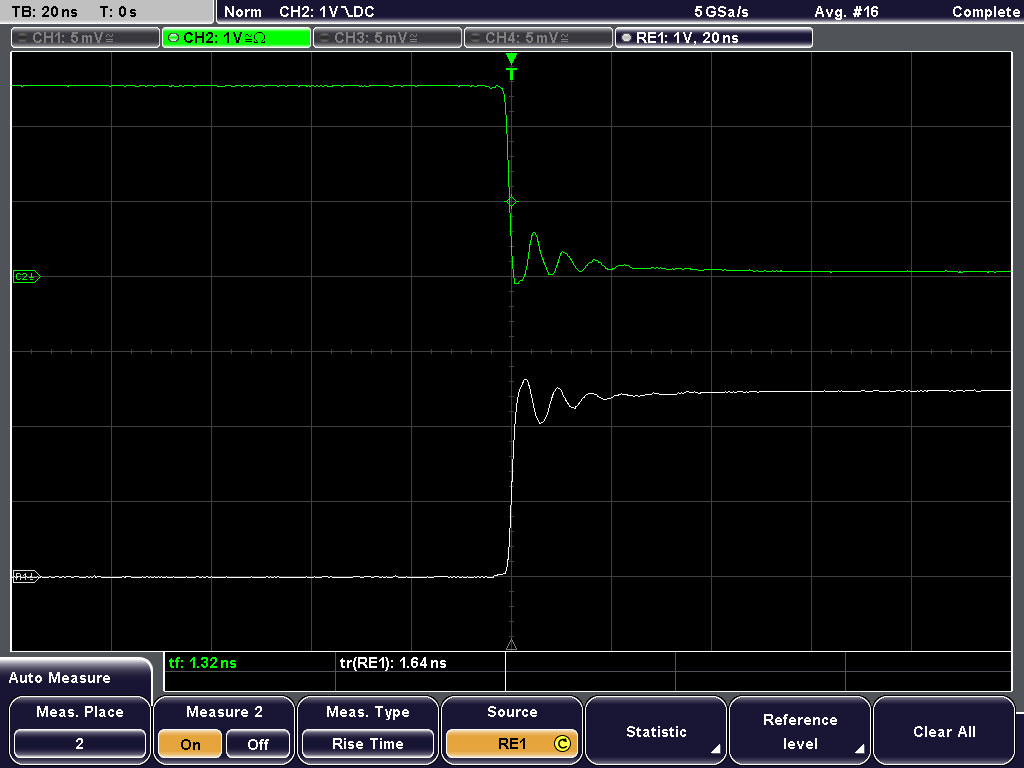
The PPS pulse output, when terminated into 50 Ω, shows a clean pulse without appreciable preshoot or overshoot. The output level is exactly 5 V open circuit.


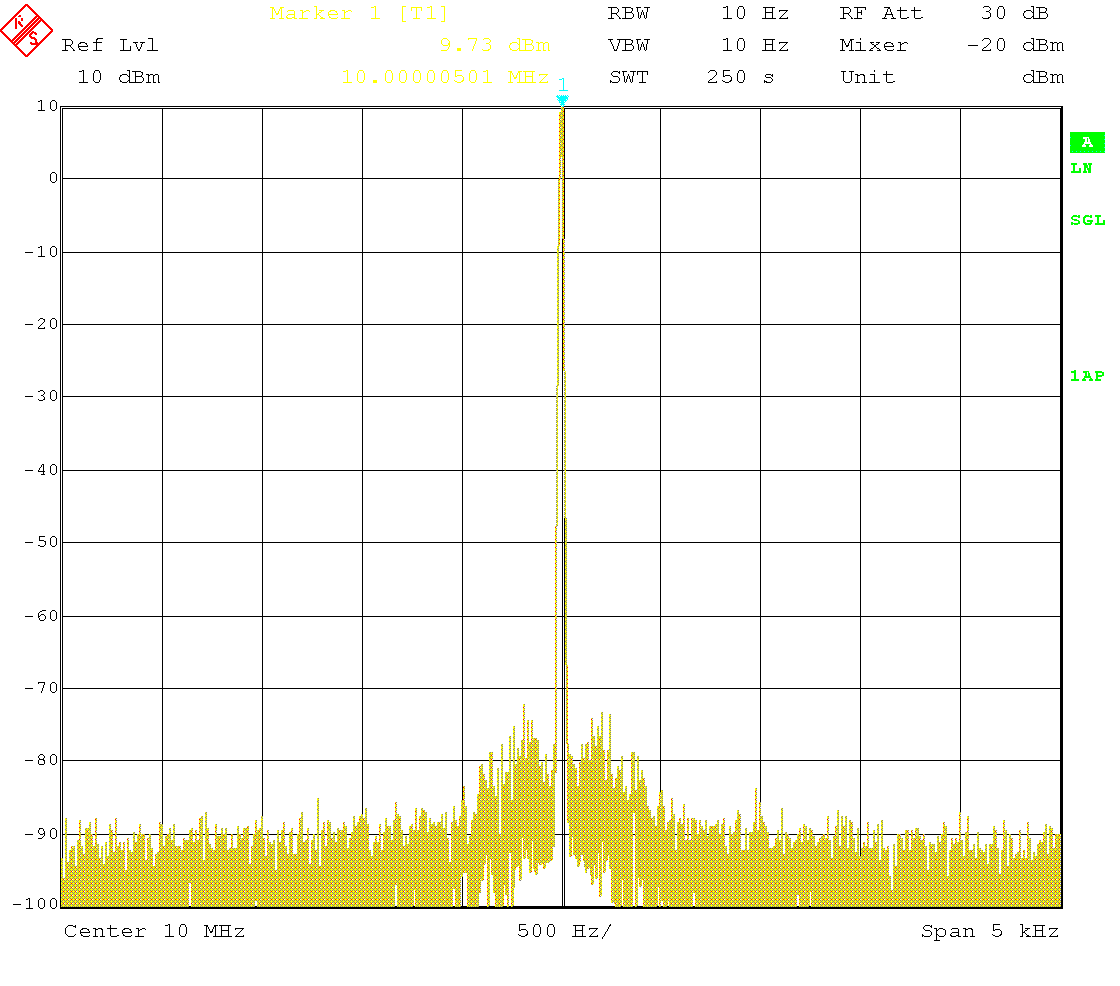
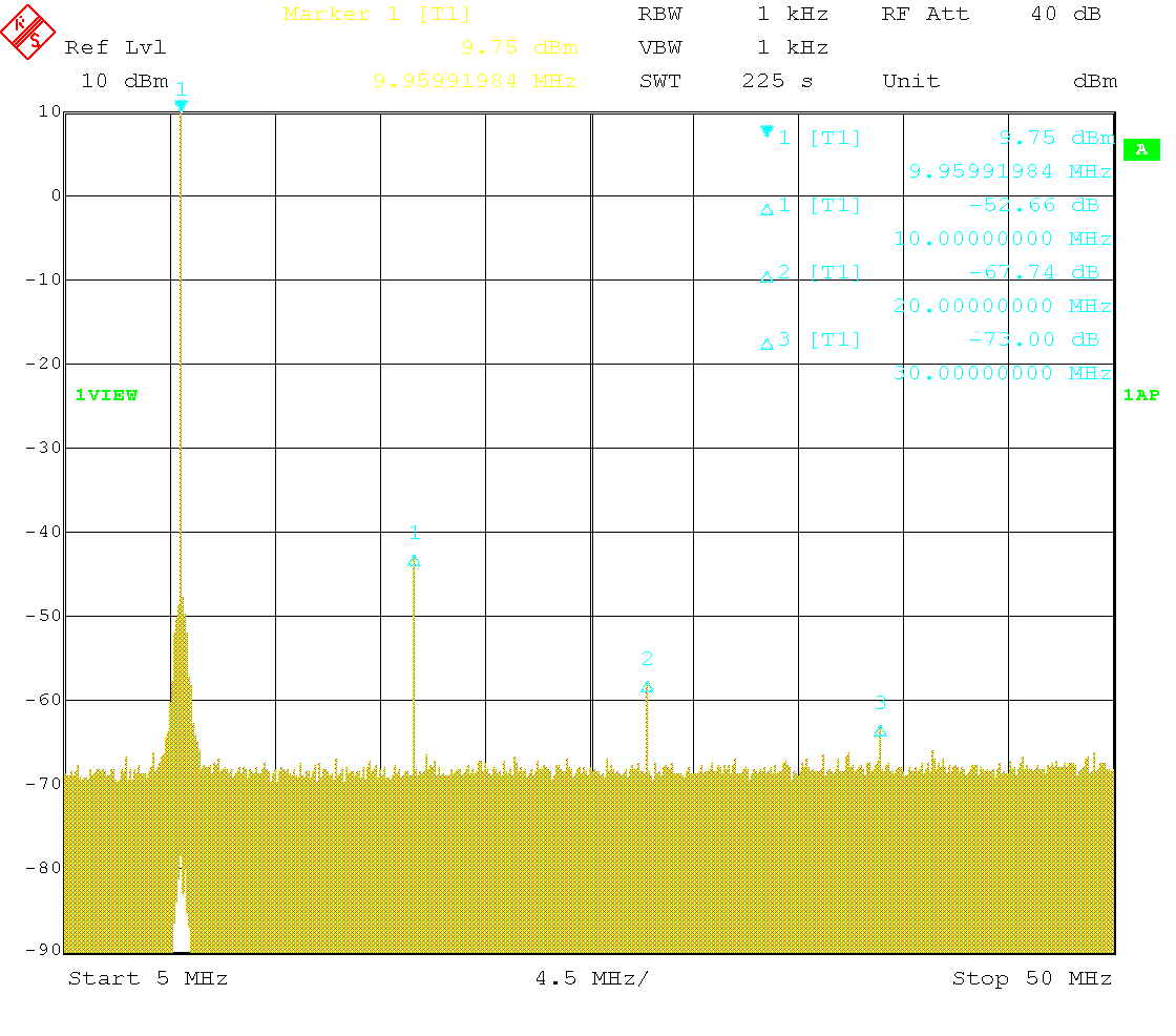
The 10 MHz sine wave outputs (10 dBm nominal level, which can be adjusted by an internal trimmer potentiometer) shows a clean carrier signal with only a small noise pedestal. The first harmonic is at less than −50 dBc, which is satisfactory for a reference frequency output. For comparison, the Stanford Research Systems Model FS735 (Option 1) Distribution Amplifier (which is equipped with an input limiting amplifier, followed by a tuned amplifier and additional filtering), has a specified THD of < 1%, which corresponds to less than −40 dB.


Frequency stability
After a few days, the brand new OCXO was still in its initial aging phase. In the first 24 h of continuous operation it has moved by ca. 30 mHz (which is compensated by the GNSS disciplining of course). An initial upward frequency drift is expected for a new OCXO and, for a healthy specimen, is supposed to become approximately linear after a few hundred days of operation [1].
The GNSS receiver was configured for a minimum survey-in period of 2 h and an accuracy limit of 15 m with the commands set:mdu 7200 and set:alm 15000. When these two criteria are met, the receiver automatically ends the survey-in period and switches to timing mode, which is indicated on the status page.
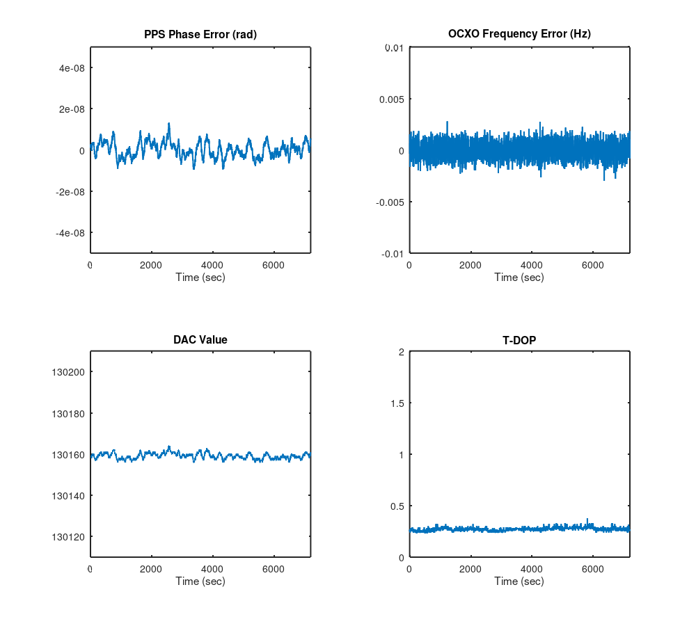

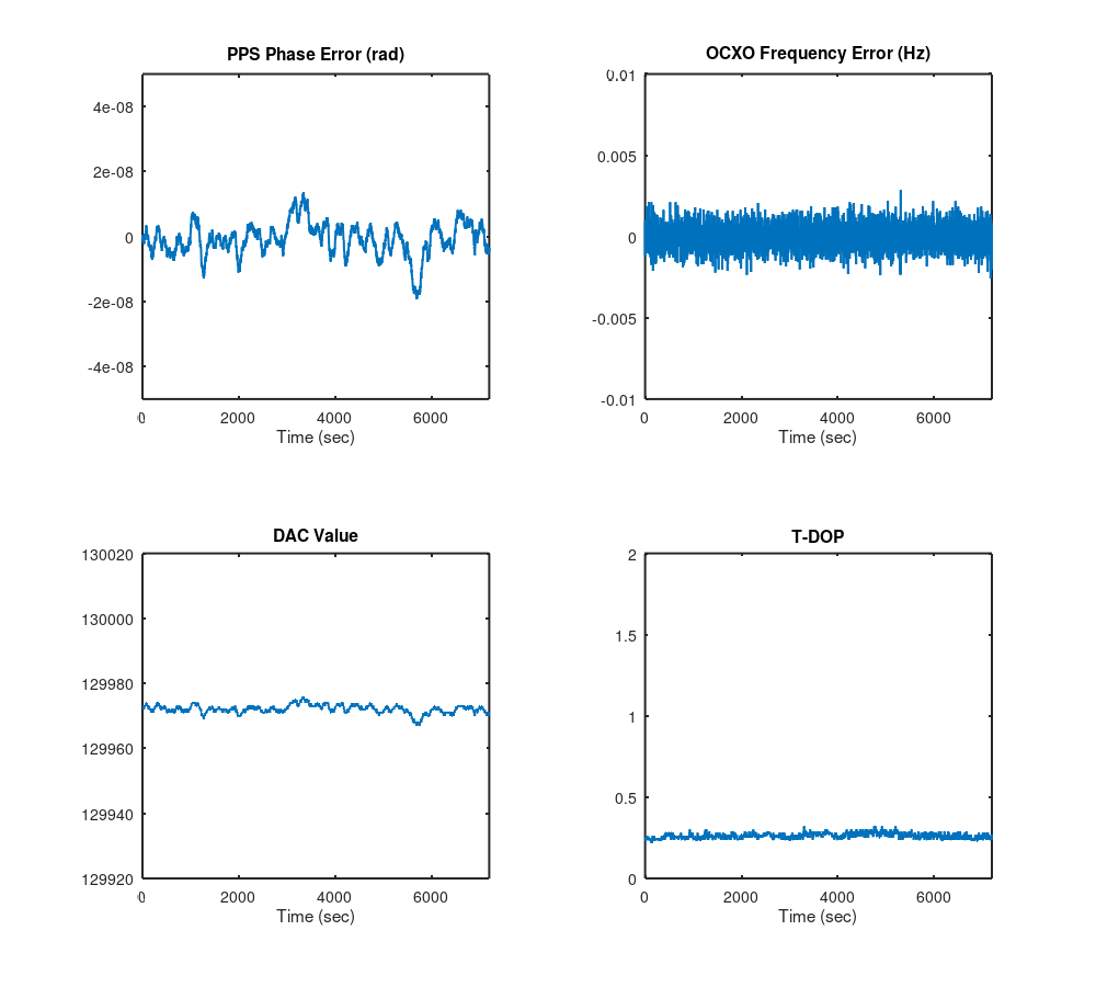

The plots above show the frequency and phase error trend as measured by the TDC over two hours for different PLL parameters ($\tau$ and $\zeta$). Also, the DAC value and the GNSS T-DOP value are displayed. At the time of data collection, the brand new OCXO had been in operation (with interruptions) for more than two months since its initial power-up. In each case the unit was running for more than 100 h before the data was taken.
Notice that these measurements are the internal ones and are affected by the GNSS time jitter (this is particularly relevant for the frequency error). Generally, it was observed that the PPS phase error measurement is sufficiently sensitive to detect even small temperature fluctuations and mechanical shocks as well as poor GNSS reception conditions and corresponding bad T-DOP values (the GNSS antenna was located inside on the windowsill, sitting on a cookie tin as a counterpoise), so sufficient settling time and a mechanically quiet environment are important.
The impact of the different PLL parameters on the control behavior can be seen. It still needs to be determined what the optimum FPLL parameters are for this particular OCXO. Also, these optimum values may change when the OCXO ages and continues to settle. It is expected to show much less short term frequency variability after about a year of operation.
Conclusion
So far, the GNSSDO seems to perform satisfactorily, also when compared with a calibrated OCXO (currently, no suitable frequency reference is in the house against which the unit could be tested). But the frequency stability still needs to be tested properly and over longer times after the OCXO has settled. Moreover, some parameters in the firmware might need tweaking, and some bugs fixing.
Addendum
An attentive reader alerted me to a bug in an earlier firmware version (missing pair of parentheses in the calculation of the loop filter coefficients). This had the effect that the time constant $\tau$ was actually smaller by a factor of $\pi$ than set, and the damping factor $\zeta$ was larger by a factor of $\pi$. This bug has been fixed in the current version.
Bibliography
- Leibfried, O., Neubig, B.: Correlation of predicted and real aging behaviour of crystal oscillators using different fitting algorithms. Download from Axtal GmbH.
