An active 10 GHz frequency tripler
For some lab experiments I needed a frequency tripler with low insertion loss and an output frequency up to 10 GHz. Since I could not find a ready-made module that meets my requirements, I designed my own, based on a Mini-Circuits RMK-3-1052+ tripler.
Mechanical construction
The tripler module is constructed on a double sided circuit board with the dimensions 71 × 34 mm that fits in a simple 37 × 74 × 20 mm shielded tinplate box supplied by Otto Schubert GmbH. The board is soldered to the box frame; SMA connectors (input, output and power) protrude through the sides as well as the lid.


Circuit design
The schematic of the module is very simple and can be viewed here as a pdf file. The complete design data including KiCad 6.0.4 schematic and board files is contained in this zip archive.
Since the circuit contains some microstrip devices and is supposed to work accurately up to over 10 GHz, it uses a special RF substrate. The substrate is the I-Tera MT40 low loss laminate made by Isola, and the board was supplied by Eurocircuits. The microstrip features assume the following data:
- Laminate thickness: 0.508 mm
- Dielectric constant: 3.38
- Loss tangent: 2.8×10⁻³
- Copper cladding thickness: 12 μm
- Copper roughness: 0.15 μm
- Copper specific resistance: 1.72×10⁻⁸ Ωm
This yields a 50 Ω microstrip trace width of 1.162 mm. The input and output SMA connectors (Cinch part no. 142-0721-881) are chosen not to introduce any impedance discontinuities with this microstrip width.
The input signal is fed into the integrated RMK-3-1052+ tripler U1, which is specified for input frequencies from 2.2 GHz to 3.5 GHz. This is also the frequency range that was assumed in the design of the circuit. There is not much information provided by Mini-Circuits about the inner workings of this tripler, only that it is based on a “specially designed diode quad ring configuration to enable high rejection of adjacent harmonics”. The tripler is followed by a microstrip high-pass filter and an GVA-123+ MMIC amplifier U2 from Mini-Circuits, based on a GaAs heterojunction bipolar transistor. The gain of the amplifier is sufficient to compensate for the insertion loss of the tripler and filter over much of the frequency band. The main purpose of the filter is the suppression of the fundamental feed-through in the tripler, which is specified to be about 2.5 dB below the third harmonic at mid band when driven with 7 dBm.
The microstrip filter is a fifth order high-pass filter with grounded stubs. It can also be considered a band-pass filter, which, as usual for microstrip devices, is to some extent a question of definition. The filter was first designed using standard filter design procedures, and then optimized with a linear S-parameter simulation with QucsStudio, using the usual microstrip models. Finally, it was fine tuned for its corner frequency and a flat pass-band with an EM simulation using OpenEMS. The EM simulation of the final result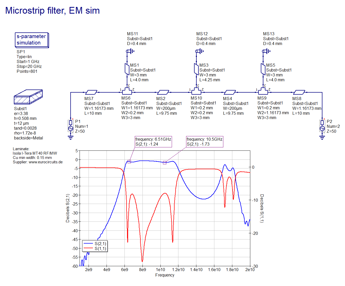 shows a very flat response with low insertion loss. Its microstrip layout
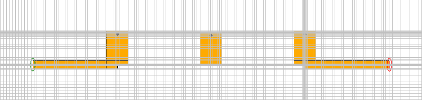 was finally re-drawn in KiCad.
The bias tee for U2 consists of two inductive transmission lines of 0.2 mm width and two radial stubs. The transmission lines were initially chosen to be λ/4 at mid band, and the opening angle of the radial stubs was chosen as 90° to achieve a good broadband response. Then this structure was optimized with an S-parameter simulation, and fine tuned with an EM simulation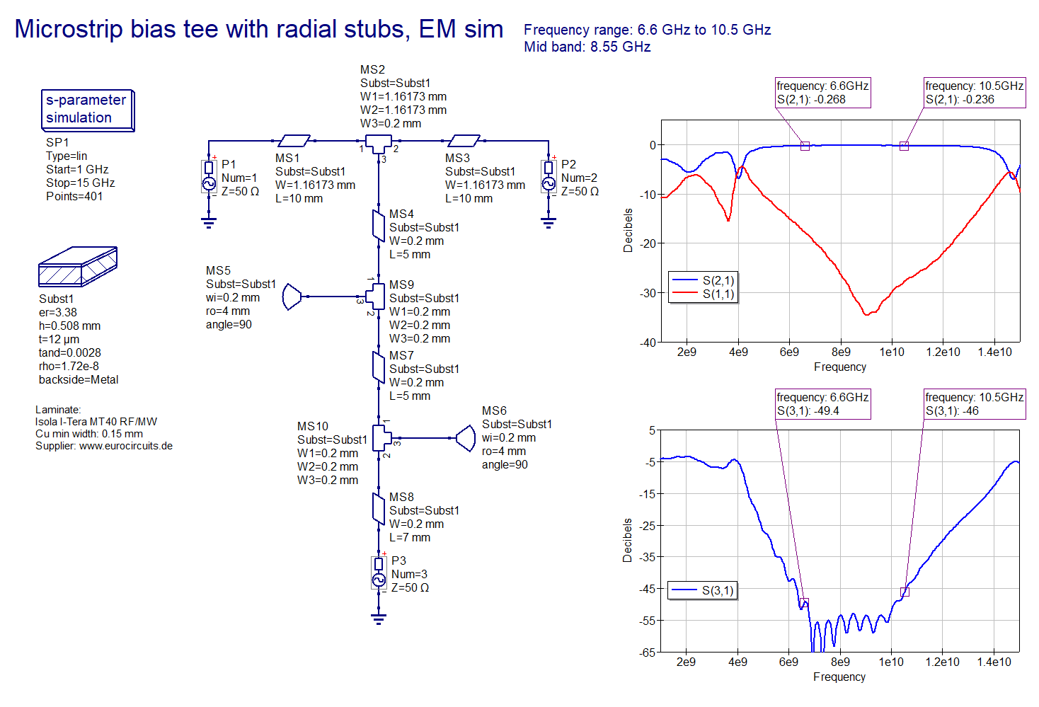 for maximum flatness in the useful band, and for good isolation of the DC port. In the final circuit, an additional choke in the DC path blocks lower frequency components. The layout of the bias tee
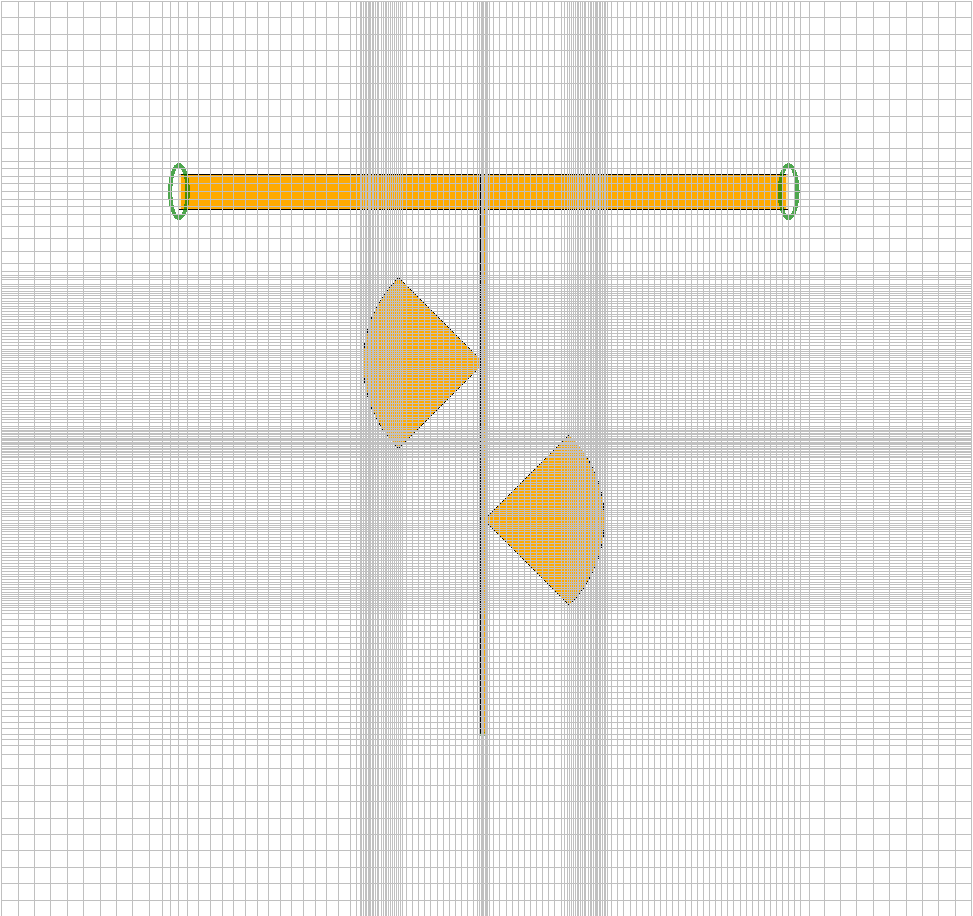 was also re-drawn in KiCad, which is very easy in the new version 6. A 3D rendering of the complete circuit board can be seen below.

For proper operation the tripler module requires 5 V DC at the SMA jack J1. The current consumption is about 68 mA. The nominal drive level at the input is 7 dBm.
Performance
Frequency response
First the output level of the third harmonic was measured over frequency for various drive levels. The result can be seen in the diagram below for drive levels of 4 dBm, 7 dBm, 11 dBm, and 13 dBm.

For the nominal drive level of 7 dBm the output level is fairly flat over frequency. Only beyond 9.2 GHz it starts to roll off slowly, which is the combined effect of U1 and U2, and is expected from their datasheets. For example, the gain of U2 alone drops by about 4 dB between 8 GHz and 10 GHz. The other level variations as well as the slight drop around 8.9 GHz are almost solely due to U1. This becomes evident by comparing the frequency response for different drive levels: flatness gets considerably worse for lower drive levels. The other circuit components and, in particular, the microstrip structures, do not contribute much to the overall level variation with frequency, as becomes evident from the EM simulations (they are very accurate for a precisely manufactured board made from an RF laminate).
Output spectrum
Next the spectrum of the output signal was measured at different frequencies across the useful frequency band. The drive level was 11 dBm in each case.


Of particular interest are the tones below the third harmonic. It can be seen that they are at least 30 dB below the wanted third harmonic.This shows that the microstrip filter is effective in suppressing the fundamental feed-through. However, the second harmonic is larger than the RMK-3-1052+ datasheet would suggest (between 50 and 60 dB below the third harmonic). Even though I have not investigated this phenomenon in detail, it is likely caused by the lack of a broadband 50 Ω termination at the output of the RMK-3-1052+: the microstrip filter is reflective in its stopband and reflects energy contained in the fundamental tone back into the tripler.
Conclusion
The measurements indicate that the tripler module performs sufficiently well for my needs. In particular, it provides a good suppression of unwanted tones in the output signal.