An experimental CW signal generator based on the ADF4351
This page describes my first attempt at designing and building a simple single board CW signal generator based on a PLL synthesizer chip with integrated VCO. It uses the Analog Devices ADF4351 integrated PLL synthesizer. Meanwhile I have built an improved version using the Texas Instruments LMX2582, which is at the same time simplified since it does not use a DDS to keep the main PLL only in integer-N mode in order to avoid integer boundary spurs.
While it is not difficult to set up a basic synthesizer with a chip like the ADF4351, the bigger problem is to achieve an output signal that has an accurately and finely adjustable level over a wide frequency range, as well as low spurs and harmonics. The present project can be considered as a first draft towards this goal. Due to the simplistic circuit and single board design using standard FR4 it turned out to be challenging, and the original goal that I set myself was not fully met. Nevertheless, this signal generator achieves an accurately leveled output up to about 3 GHz at −20 dBm, and up to 2 GHz at 0 dBm, but unfortunately it has an increased spur level beyond 2 GHz due to an interesting problem with a wideband amplifier—see below. By adding some circuit complexity and modifying some aspects, this design could be used as the basis of a fairly capable signal generator.
Mechanical construction
Let's start with the mechanical construction, as it sets some limits for the complexity of the circuit. The signal generator is built on a single four layer board with the dimensions 220×160.5 mm. The board is lightly populated to facilitate easy manual assembly and soldering. It is housed in a Hammond model 1455 R 2201 enclosure.


The front and rear panels have been manufactured by Schaeffer AG from Berlin, using their software “Frontplatten-Designer”. The board was designed with KiCad version 5.1.6 and manufactured by JLCPCB with their impedance controlled process using prepreg type 7628. The board layout assumes the the following data:
- Prepreg thickness: 0.2 mm
- Prepreg dielectric constant: 4.60
- Outer layer copper thickness: 35 μm
According to the standard approximation formulas this leads to a 50 Ω microstrip trace width of about 0.349 mm. The top layer of the board is used for RF signals, whereas the bottom layer contains all non-RF control signals; the inner layers are used for ground and power.
Circuit diagram and design data
The schematic of the signal generator consists of seven pages and can be viewed here as a pdf file. The complete design data including KiCad schematic and board files, Gerber files, the firmware source code (written in C), and the front and rear panel artwork, is included in this zip archive. Hopefully, the source code is sufficiently commented to be comprehensible.
Circuit description
The signal generator uses a “headless” design without front panel controls. It is operated via a USB interface, which establishes a virtual COM port. For basic control of the generator a simple terminal program is enough, even though this is not very convenient. It would be better to create some software with a graphical user interface, even though I have not gone to this effort. The USB port is handled by U22, which is a FT230XS USB to UART interface by FTDI. It is connected to microcontroller U23, a Microchip (Atmel) ATmega4809-A, which is the brains of the generator and controls all other devices on the board, either via SPI or directly through GPIO lines.
The microcontroller U22 is connected to two general purpose debug LEDs on the main board, which can be useful for firmware development. There are three further LEDs, which indicate lock of the main and reference PLLs, as well an output unleveled condition. Moreover, there are two LEDs which indicate transmit and receive activity on the USB interface. A single front panel status LED is provided; it lights green during normal operation, and red when an error occurs (e.g. a loss of lock of one of the PLLs, the output being unleveled, an argument of a received command being out of range, etc.). Another test facility is a loopback test of the USB data link, which can be enabled by placing a jumper.
Frequency processing starts from the internal reference U6, an accurate 10 MHz TCXO by Connor-Winfield. Then U3, an ultra-low phase noise VCXO running at 100 MHz is phase locked to the reference frequency by means of integer-N PLL chip U4, which is an ADF4002 from Analog Devices. It contains RF and reference frequency dividers, a phase-frequency detector, a charge pump, and lock detect circuitry. The VCXO is a CVHD-950X-100.00 by Crystek; it features a HCMOS output and a phase noise floor of about −166 dBc/Hz. Resistors R6, R8, R9, R10 and R17 set the appropriate signal levels. The loop bandwidth of the reference PLL is adjusted to about 50 Hz with 50 degrees of phase margin by the three-pole loop filter C30, C31, R13, R7, C32 and C33. In this way the low phase noise of the VCXO is not impaired by the reference, even close to the carrier. Provision is made to connect an external reference frequency. The external reference signal is conditioned by U2A and routed to the reference input of U4 when commanded by the microcontroller. Resistor R11 and diodes D3 and D4 protect the external reference input.
The phase locked 100 MHz signal from the VCXO is fed to U11, an AD9951 by Analog Devices. This is a 14-bit DDS synthesizer featuring a 32-bit tuning word and a current output DAC. To optimize phase noise, the internal reference multiplier PLL of U11 is disabled, and the 100 MHz is directly used as DDS system clock. The current output of U11 is converted to a single-ended voltage by R21, R22, and transformer T2, and then passed through the reconstruction filter, a steep Cauer filter with a corner frequency of 45 MHz and 80 dB attenuation. The DDS output in this application is 35 MHz at maximum, thus the first image is at $100\,{\rm MHz}-35\,{\rm MHz}=65\,{\rm MHz}$, which the filter attenuates, in theory assuming ideal components, by about −57 dB, plus the attenuation due to the $\sin(\pi fT)/\pi fT$-roll-off from the zero order hold transfer function of the DAC, which is about 7.2 dB, where $T=1/f_\text{sysclk}$ is the system clock period.
The DDS output is used as reference input for U10, the ADF4351 wideband synthesizer with integrated VCO by Analog Devices. Its VCO, which really is a set of three separate VCOs, each with 16 overlapping frequency bands, operates between 2.2 GHz and 4.4 GHz, with additional divide-by-$2^a$ circuits, where $a=0,\ldots,6$. Thus frequencies between less than 35 MHz and 4.4 GHz can be generated. The firmware in microcontroller U23 will keep the VCO frequency as low as possible for a given output frequency in order to minimize phase noise. Moreover, to avoid integer boundary spurs the internal PLL of U10 is solely operated in integer-N mode. Depending on the output divider setting this will lead to large frequency steps, therefore fine tuning is achieved by modifying U10's reference frequency by means of the DDS synthesizer. The DDS output is directly fed to the phase-frequency detector (PFD) of U10, all internal reference dividers and doublers are disabled. Thus near an output frequency of 4.4 GHz, with a DDS system clock of 100 MHz, a PFD frequency of about 35 MHz and a 32-bit DDS tuning word this will lead to a frequency resolution of \[\frac{4.4\cdot10^9\,{\rm Hz}}{35\cdot10^6\,{\rm Hz}}\times2^{-32}\times100\cdot10^6\,{\rm Hz}\approx2.93\,{\rm Hz}.\] With output dividers enabled and at lower VCO frequencies, the frequency resolution at the output will be, of course, lower. The three-pole loop filter C101, C102, C103, R209 and R30 of the internal PLL of U10 has a bandwidth of 120 kHz, and the PLL charge pump current is set to 5 mA. Further settings of U10 can be seen in the source code (refer to file hw_control.c and the comments therein).
The output of U10 is further amplified by U9, an ADL5565 high dynamic range differential amplifier by Analog Devices, and then converted to a single ended signal by transformer T1, which also achieves some voltage gain. Next in the singal path is the voltage controlled attenuator, which is realized by D6, a quad pin diode from M/A-COM. This voltage controlled attenuator is part of the automatic level control circuitry.
The voltage controlled attenuator is followed by an 8-band harmonic filter bank. The individual low-pass filters are switched by U12 and U13, both HMC321ALP4E GaAs SP8T RF switches by Analog Devices (formerly a Hittite part). There is also a bypass line, which is switched by U14 and U15, two GaAs SPST switches from Analog Devices (formerly a Hittite part), whose inputs are opens when off. The filters are switched automatically by microcontroller U23, depending on the output frequency. The following table lists the corner frequency and frequency range of use for each filter:
| Band | Corner freq. (MHz) | Output range (MHz) |
|---|---|---|
| 1 | 60 | 35 … 60 |
| 2 | 100 | 60 … 100 |
| 3 | 180 | 100 … 170 |
| 4 | 300 | 170 … 290 |
| 5 | 520 | 290 … 490 |
| 6 | 880 | 490 … 830 |
| 7 | 1500 | 830 … 1400 |
| 8 | 2500 | 1400 … 2400 |
| at output | 4800 | 2400 … 4400 |
The filters of band 1 to 6 are realized as lumped component LC filters. After designing them they have been built on a test board and tweaked while measuring them with a network analyzer. The filters of band 7 and 8 are realized as microstrip stepped impedance filters; they have also been tested with a network analyzer. Further down the signal path is another 4.8 GHz stepped impedance low-pass filter. It serves as harmonic filter when bypass is selected (above 2.4 GHz output frequency), and it also attenuates unwanted high frequency output at the output of the filter bank.
The final low-pass filter is followed by U16, a GVA-84+ MMIC amplifier from Mini-Circuits. This amplifier has a 1 dB compression point of about 20 dBm at 4 GHz. It is followed T3, a RBDC-20-63+ power signal tap from Mini-Circuits. This resistive device with very low insertion loss has a coupling ratio of about 20 dB and taps off a sample of the signal after U16, which is further attenuated by 15 dB by means of a MMIC attenuator (HMC657LP2E by Analog Devices) for use by the level detector U19, an AD8319 by Analog Devices. This level detector is part of the automatic level control (ALC) circuitry. After T3, the RF resistor R45 sets the output impedance to 50 Ω.
The ALC control loop is closed within level detector U19, which compares the detected voltage, proportional to the signal level after U16, with the level setting voltage at pin 7 of U16, which is supplied by DAC U25. Between the output of U19 and the voltage controlled attenuator D6 is the low-noise rail-to-rail op amp U20, which shifts the output voltage to the range from 0 V to 5 V, and also sets the ALC bandwidth to approximately 10 Hz. Comparators U21 detect if the output signal is unleveled. This condition is monitored by microcontroller U23.
Further down the signal path, after T3 and R45, follows the digitally controllable GaAs MMIC step attenuator U17, which is a HMC629ALP4E by Analog Devices (formerly a Hittite part). This attenuator can be set between 0 dB and 45 dB in steps of 3 dB. It is used for coarse level setting, and is under automatic control of microcontroller U23. Fine control of the output level is done by U25, a 12-bit DAC, also controlled by U23. Frequency dependent level correction by means of a calibration table stored in the internal EEPROM of U23 is performed automatically by both the DAC U25 and the step attenuator U17.
The generator is operated from a DC voltage of approximately 6 V to 16 V, supplied to a rear panel barrel jack. Two low dropout linear regulators U26 and U27 generate stable 5 V and 3.3 V for noise critical analog circuitry, whereas regulators U29 and U30 generate 3.3 and 1.8 V for digital circuitry. Noise critical components such as VCXO U3, or the VCO in U10, have their own local low-noise linear regulators U1, U7, and U8, which are LT3042 by Analog Devices (a former Linear Technology part).
Operation
As was explained above, the signal generator is operated via a USB interface, which establishes a virtual COM port. In the following, the protocol for controlling the generator is briefly described.
All commands consist of three capital letters. There are two kinds of commands: Setting commands, which have a numerical argument, and interrogation commands, which end with a question mark. The signal generator responds to an interrogation command by sending a string. A string consisting of a command and an argument, or a command and a question mark, must be followed by a newline and/or carriage return character to start execution. Arguments are integer only, no decimal point is allowed. A newline and/or carriage return character flushes the receive buffer. Invalid commands are ignored. Arguments outside permissible bounds generate an error.
The serial interface expects data at 56000 baud, with 8 data bits, one stop bit, and even parity. It sends data with the same parameters. The following table lists all commands.
| Command | Description |
|---|---|
| INF? | Get info string (Signal Generator, Dr. Mario Hellmich, Salzgitter) |
| VER? | Get firmware version |
| ERR? | Get binary error code, zero means “no error”, also clears the last “argument out of range” error |
| FRQ? | Get current output frequency in Hz |
| LVL? | Get current output level in multiples of 0.1 dBm |
| FRQ [frq] | Set output frequency to frq (from 35000000 to 4400000000, in Hz) |
| LVL [lvl] | Set output level to lvl (from −450 to 100, in units of 0.1 dBm) |
| REF? | Get reference status (0: internal, 1: external) |
| REF [sts] | Set reference status (sts=0: internal, sts=1: external) |
| RFQ? | Get reference multiplier |
| RFQ [mul] | Set reference multiplier to mul (from 10 to 255) |
| SVE [mem] | Save current setup to memory mem (from 0 to 9, generator will always start up from state in memory 0, even when USB is not connected) |
| RCL [mem] | Recall setup from memory mem (from 0 to 9) |
| LCR? | Get level correction value for current frequency |
| LCR [cor] | Set level correction value for current frequency to cor (from −5000 to +5000, in multiples of 0.01 dB) |
| FCR? | Get correction value for internal reference in Hz |
| FCR [cor] | Set correction value for internal reference to cor (from −1000 to +1000, in Hz) |
| SCR? | Get slope correction value for level detector, in multiples 0.01 mV/dB |
| SCR [cor] | Set slope correction value for level detector to cor (from −30000 to +30000, in multiples of 0.01 mV/dB) |
Here are some examples: Sending “FRQ 1500000000\r\n” sets the output frequency to 1.5 GHz. Sending “LVL −100\r\n” sets the output level to −10 dBm. Sending “REF 0\r\n” selects the internal reference.
The reference multiplier works as follows. For an external reference signal with frequency $f$, the reference multiplier $m$ must be set such that $f\cdot m=100\,{\rm MHz}$. For example, when a 5 MHz signal is to be used as external reference, send “RFQ 20\r\n”.
The calibration values for the internal reference, the output level, and the detector slope, as well as ten instrument setups (consisting of output frequency and level, internal/external reference, and external reference multiplier) are stored in the internal EEPROM of microcontroller U23. The firmware is parametrized for 44 level calibration points between 35 MHz and 4.4 GHz, i.e., one point every 100 MHz. The correction value that the LCR? or LCR [cor] commands refer to is determined by the current output frequency. For example, if the output frequency is 123.456 MHz, the current correction value is 100 MHz. To set the level correction value at, for example, 100 MHz, set generator to that frequency, measure output level, and set correction value with “LCR [cor]\r\n” accordingly.
Performance
Spectral purity near the carrier
First let's take a look at the spectrum in the vicinity of the carrier. The result for carrier frequencies of 100 MHz, 1 GHz, 2 GHz and 3 GHz, and at an output level of −20 dBm, can be seen in the following pictures. All spectra have been measured with 100 Hz resolution bandwidth and 20 Hz video bandwidth, and with the auto peak detector. I have not included a spectrum at 4 GHz since the output leveling circuitry starts to run out of steam above 3.3 GHz. The output level will reach almost −20 dBm at that frequency, but the level control range is already exhausted—see below.


The same spectra but recorded with the sampling detector and endowed with phase noise markers can be seen here for carrier frequencies of 100 MHz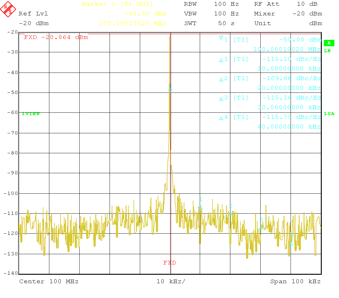 , 1 GHz
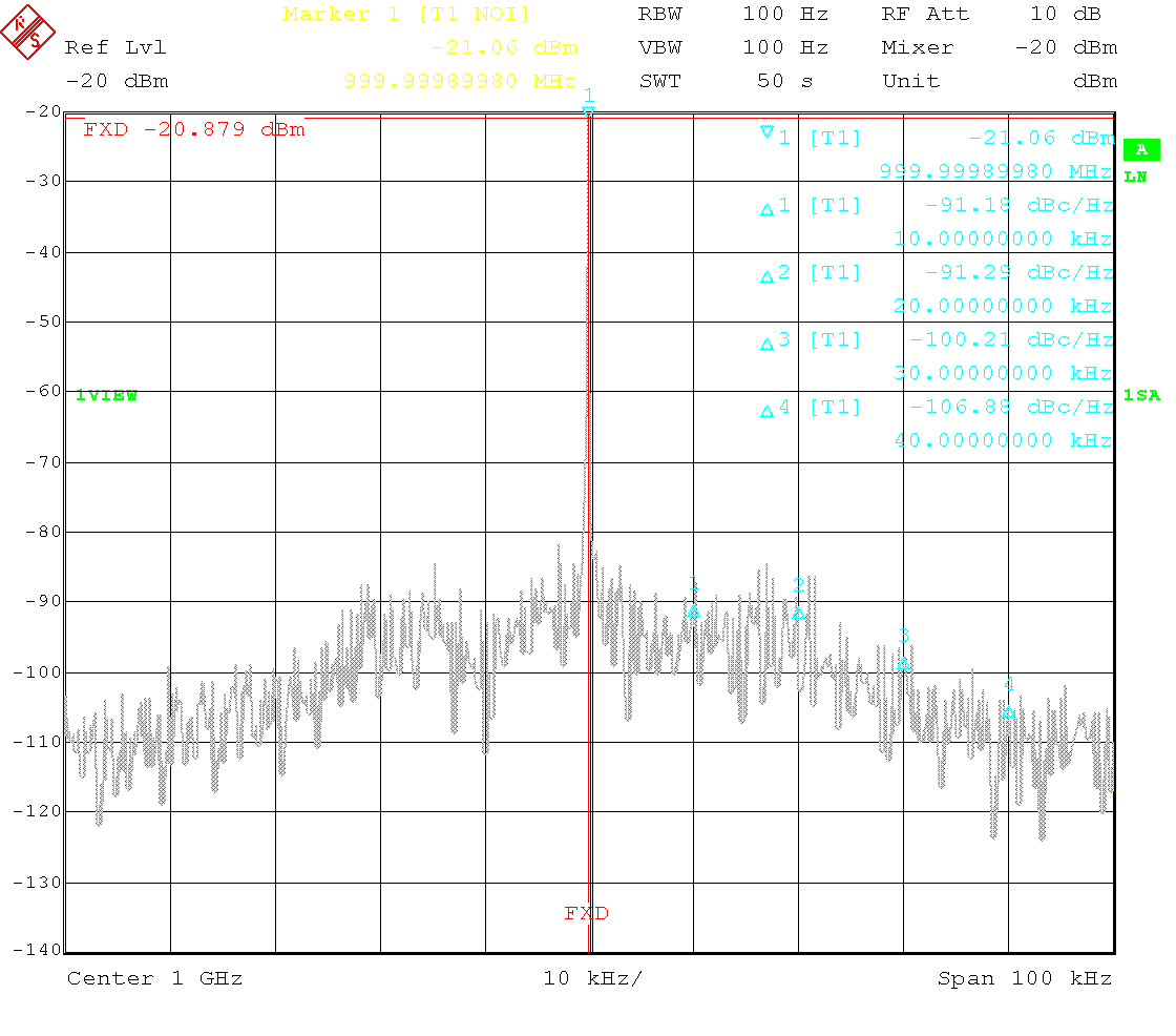 , 2 GHz
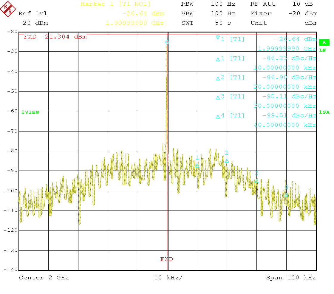 , and 3 GHz
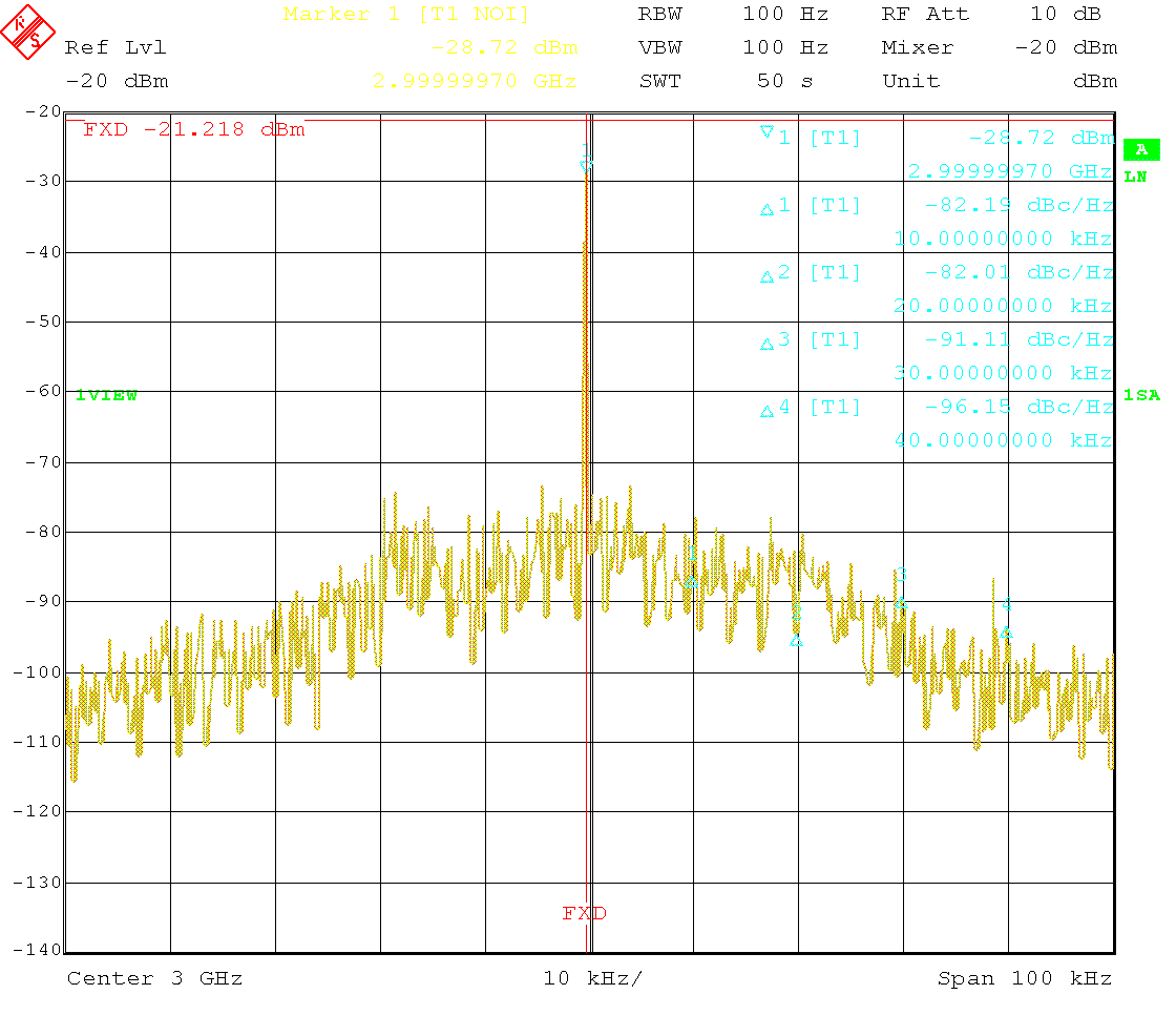 .
.
Notice that the phase noise markers indicate a somewhat worse phase noise performance that the datasheet values of the ADF4351 suggest. First this is because the datasheet assumes ideal conditions, and here the device is operating as part of a complicated circuit (for example, the DDS synthesizer as a reference is not as clean as a good crystal oscillator, and there is an influence of the signal path downstream of U10). Moreover, these phase noise figures were determined with a spectrum analyzer, which indicates total noise, and not exclusively phase noise (it will not reject amplitude noise).
Harmonics and spurs
Next we look at the harmonic and spurious content at the output for various carrier frequencies. In particular, these indicate the performance of the harmonic filters.


Looking at the harmonics one reads off a harmonic suppression of about 43 dB of the first harmonic for a 1 GHz carrier. For all other carrier frequencies shown the harmonics are suppressed by about at least 60 dB. Checking some other carrier frequencies shows that these numbers are consistent. The signal generator thus achieves excellent harmonic suppression. Therefore, the output signal appears as a perfect sine on an oscilloscope, as seen here at 50 MHz and +5 dBm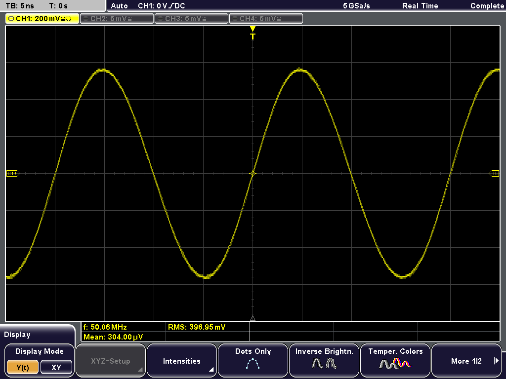 with a scope bandwidth of 500 MHz.
Unfortunately there are some pronounced spurs that tend increase with output frequency. Some are due to the phase-frequency detector in U10. The datasheet specifies a suppression of phase-frequency detector spurs of about 80 dBc, but the downstream circuity increases them markedly. See the discussion below for further details.
Output leveling
Output level accuracy is determined by the level correction values stored in the EEPROM of U23. The firmware uses a total of 44 calibration points between 35 MHz and 4.4 GHz, i.e., one point every 100 MHz, with linear interpolation between the points. One could increase the number by changing a parameter in the source code, however, the EEPROM size will set a limit to the number of calibration points (current EEPROM usage is about 44%).
The level accuracy was measured by sweeping the generator from its minimum to its maximum frequency. This was achieved by controlling it by a GNU Octave script, using the Octave Forge instrument control package. This script is available for download. Running this script and recording the level with a spectrum analyzer set to max hold yields the following result.

It can be seen that the maximum level of 10 dBm that can be set is only maintained up to about 2 GHz (the unleveled error will already be issued from 620 MHz onward, meaning the voltage controlled attenuator is very near its end stop). At −10 dBm the generator is fully leveled up to over 2 GHz, and at −20 dBm up to over 3 GHz (the proper level is maintained a bit beyond that point, but the generator indicates an unleveled condition).
The level correction values have been calibrated with a diode power sensor directly connected to the output. The spectrum analyzer, however, was connected by a cable, and had a DC block at its input jack, therefore the level reads a little lower towards higher frequencies. Moreover, one can see the individual calibration points every 100 MHz, and a slight drop between them.
The 0 dBm trace shows one dip near 1.5 GHz where the generator becomes briefly unleveled; this is due to a resonance in the bias network L32, L33, C207 and C203 of amplifier U16, as has been verified by a network analyzer. The spikes seen on the −20 dBm trace are due to switching glitches, which are recorded by the analyzer in max hold mode. They are absent during stationary operation.
The maximum output level obtainable when setting the generator to 10 dBm is shown in the following measurement. Superimposed on the roll-off towards higher frequencies due to various losses, some dips can be seen. These are due to the harmonic filters, which should be a little wider.

Settling time
The settling time after frequency or level changes depends on the magnitude of the frequency or level change. Below are shown some examples of frequency changes.


The measurements show settling times of less than about 1.5 ms for the synthesizer, the ensuing level correction takes somewhat longer due to the narrow bandwidth of the ALC loop. This is not fast, but acceptable. In the design of this generator, no provisions have been made to achieve a fast locking PLL or low ALC settling time. The ADF4351 offers some facilities for fast lock. By using them, speeding up the ALC loop, and using a faster microcontroller, a much more frequency agile generator could be achieved.
Some design considerations
With only two amplifier stages (U9 and U16) after the synthesizer U10 with integrated VCO, it is clear that the maximum achievable output level will compromised in this design. Nevertheless, I did not expect that the frequency dependent losses are so big that 10 dBm output level can only be maintained up to 1 GHz, and −10 dBm only up to 2 GHz. The main origins of loss are the voltage variable attenuator (up to 6 dB), the harmonic filters (up to about 10 dB), various coupling capacitors (there are ten after U9 when the filter bypass is selected), as well as the circuit board.
Building microstrip filters on cheaply manufactured FR4 boards is challenging. For this reason, the bandwidth of the stepped impedance filters is somewhat too small, as can be seen in the following picture, which shows the S21-magnitude of the 4.8 GHz filter at the output of the harmonic filter bank.

The next picture shows the S21-magnitude of the voltage variable attenuator for various control voltages between 0 V and 5 V. Moreover, S11 and S22 are shown for 0 V (outer curve, maximum attenuation) as well as 5 V (inner curve, minimum attenuation).

Amplifier U9 has given me a lot of trouble. It tends to be unstable and oscillates at output frequencies around 490 MHz. As a quick fix a THT resistor has been added to its input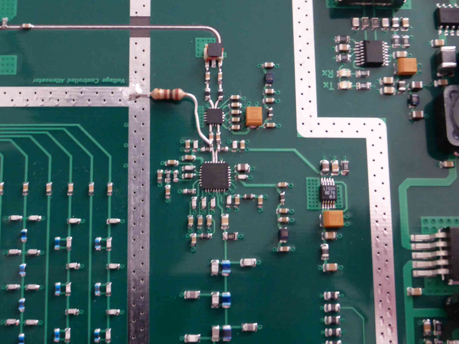 , which stopped the oscillation.
But this is not the only problem with this amplifier. As has been mentioned above, it is responsible for the increased spurs below about 800 MHz at output frequencies from 2 GHz onward. These spurs are probably due to U9 being driven into compression, which it does not seem to like. I have not yet fully understood the nature of these spurs, but they could be due to a parametric instability of this amplifier, which is excited by spurs at the output of U10, which originate from the phase-frequency detector. (No, they are not due to the added THT resistor.) See this close-up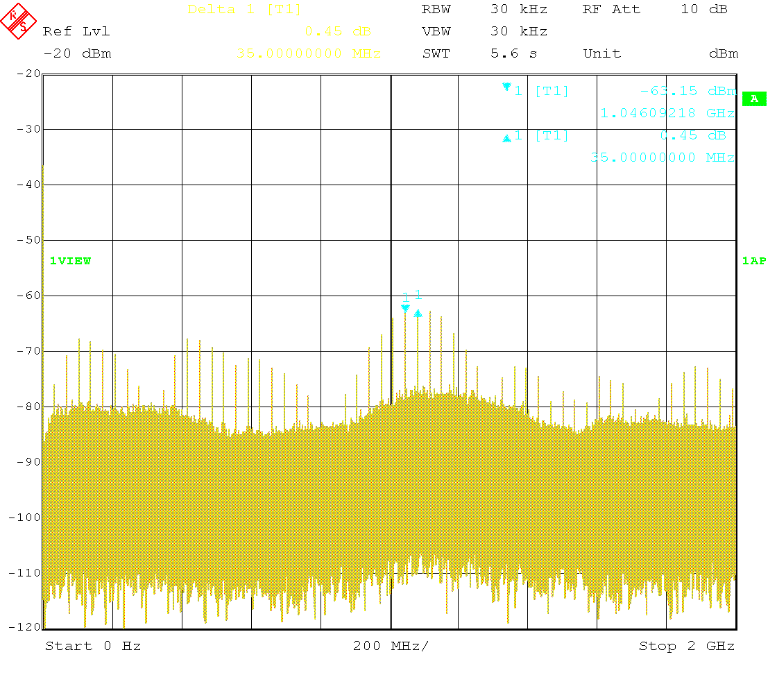 of the spurs at the generator output. As the following picture indicates, it is not the ADF4351 which is at fault here. The picture shows the output signal right after C68, with U9 removed, and a coaxial cable soldered to the right hand side of C86. The phase-frequency detector spurs can be seen, but they are measured to be about 77 dB below the carrier, which is acceptable (the datasheet value is 80 dB). Also note that for this measurement the spectrum analyzer was connected with a rather long piece of cheap RG174 cable soldered directly to the board, which is expected to have a couple dB loss at 3 GHz, so the datasheet value is probably exceeded.

To be fair, it must be mentioned that U9 is operated beyond its specifications in this application. The datasheet states that the output voltage swing × bandwidth product of the ADL5565 must be below 2000 Vpp×MHz. This is exceeded at higher frequencies. In retrospect it was not a wise decision to employ this amplifier here. Instead, one should have used a wideband transformer directly at the output of U10 to convert to a single ended signal, followed by a MMIC or FET amplifier.
Conclusion and possible improvements
The two main problems with this design are the rather low maximum output level and the spurs due to the problems with amplifier U9. They can be addressed by redesigning the circuitry around U9 as explained above, and by adding some more gain into the signal path following the synthesizer chip. Moreover, some efforts to minimize losses would help, which would also make it easier to achieve a flatter output level between the calibration points.
Other than that, the generator performs satisfactorily, and is a good starting point for a more refined design. A redesign would also be an opportunity to make provisions for a fast locking PLL, which would give the generator the capability to do faster frequency sweeps.